Manufacturing method capable of improving plane VDMOS gate-oxide breakdown
What is AI technical title?
AI technical title is built by PatSnap AI team. It summarizes the technical point description of the patent document.
A manufacturing method and planar technology, applied in semiconductor/solid-state device manufacturing, electrical components, circuits, etc., can solve the problem of gate oxide breakdown reduction and achieve simple results
Inactive Publication Date: 2018-06-22
CHONGQING ZHONGKE YUXIN ELECTRONICS
View PDF8 Cites 4 Cited by
Summary
Abstract
Description
Claims
Application Information
AI Technical Summary
This helps you quickly interpret patents by identifying the three key elements:
Problems solved by technology
Method used
Benefits of technology
Problems solved by technology
Based on the characteristics of the planar VDMOS process, although the conventional polysilicon oxidation process or annealing treatment with oxygenatmosphere avoids the problem of impurityprecipitation in the high-temperature process of heavily doped polysilicon, it leads to the reduction of gate oxide breakdown.
Method used
Image
Click on the blue label to locate the original text in one second.
Reading with bidirectional positioning of images and text.
Examples
Embodiment 1
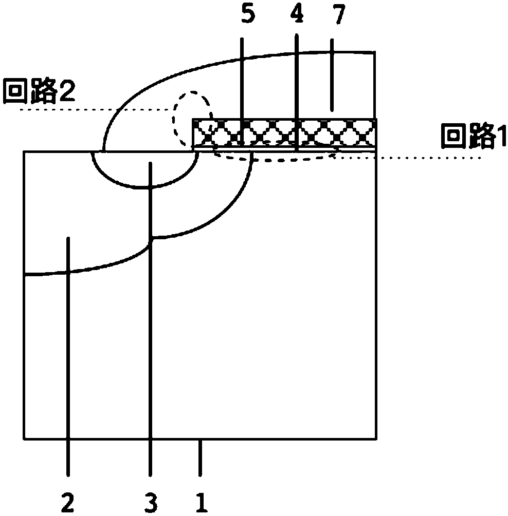
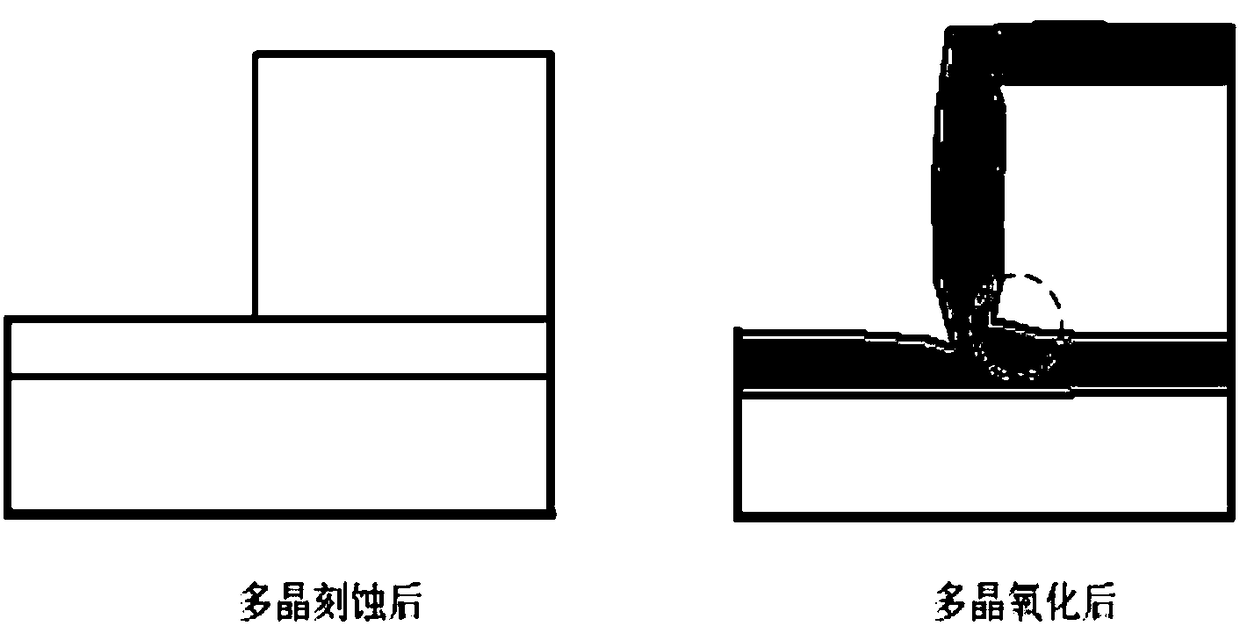
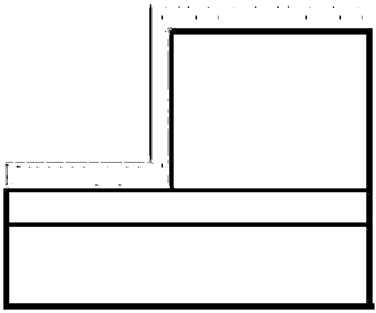
[0038] A manufacturing method for improving planar VDMOS gate oxide breakdown, characterized in that it includes an epitaxial layer 1, a well region 2, a source region 3, a gate oxide layer 4, a polycrystalline layer 5, a polycrystalline conformal dielectric layer 6, and a dielectric layer 7 and metal layer 8.
[0039] Do the following steps:
[0040] 1) The epitaxial layer 1 is formed using a conventional method.
[0041] 2) Prepare well region 2 and source region 3 .
[0042] The well region 2 is located in the epitaxial layer 1 , and the upper surface of the well region 2 is coplanar with the upper surface of the epitaxial layer 1 . The source region 3 is located in the well region 2 , and the upper surface of the well region 2 is coplanar with the upper surface of the epitaxial layer 1 .
[0043] 3) Depositing the gate oxide layer 4 .
[0044] The gate oxide layer 4 covers the upper surface of the epitaxial layer 1 . The gate oxide layer 4 also covers part of the surf...
Embodiment 2
[0057] A manufacturing method for improving planar VDMOS gate oxide breakdown, characterized in that it includes an epitaxial layer 1, a well region 2, a source region 3, a gate oxide layer 4, a polycrystalline layer 5, a polycrystalline conformal dielectric layer 6, and a dielectric layer 7 and metal layer 8.
[0058] Do the following steps:
[0059] 1) The epitaxial layer 1 is formed using a conventional method.
[0060] 2) Prepare well region 2 and source region 3 .
[0061] The well region 2 is located in the epitaxial layer 1 , and the upper surface of the well region 2 is coplanar with the upper surface of the epitaxial layer 1 . The source region 3 is located in the well region 2 , and the upper surface of the well region 2 is coplanar with the upper surface of the epitaxial layer 1 .
[0062] 3) Depositing the gate oxide layer 4 .
[0063] The gate oxide layer 4 covers the upper surface of the epitaxial layer 1 . The gate oxide layer 4 also covers part of the surf...
PUM
Property
Measurement
Unit
Thickness
aaaaa
aaaaa
Thickness
aaaaa
aaaaa
Thickness
aaaaa
aaaaa
Abstract
The invention discloses a manufacturing method capable of improving plane VDMOS gate-oxide breakdown. The method is characterized in that the method comprises an epitaxial layer, a well region, a source region, a gate oxygen layer, a polycrystalline layer, a polycrystalline shape-preserving dielectric layer, a dielectric layer and a metal layer. The method comprises the following steps: 1) formingthe epitaxial layer through a conventional method; 2) preparing the well region and the source region; 3) carrying out deposition of the gate oxygen layer; 4) carrying out polycrystalline layer deposition and doping; 5) carrying out polycrystalline lithography; 6) forming the polycrystalline shape-preserving dielectric layer through a mode of low-temperature LPCVD of SiO2, wherein the thickness of the polycrystalline shape-preserving dielectric layer is 10nm-60nm; 7) carrying out deposition of the dielectric layer through a conventional method; 8) carrying out hole lithographyetching and interconnectionmetalsputtering; and 9) carrying out interconnectionmetallithography and alloy.
Description
technical field [0001] The invention relates to the field of semiconductor power devices, in particular to a manufacturing method for improving planar VDMOS gate oxide breakdown. Background technique [0002] Vertical double-diffusionpower MOSFET (VDMOS: Vertical Double-diffusionMetalOxideSemiconductor) device is widely used in motor speed regulation and inverter due to its advantages of low power consumption, fast switching speed, strong driving capability, and negative temperature coefficient. , electronic switches, automotive electrical appliances and electronic ballasts, etc., are one of the core components of power integrated circuits and power integrated systems. [0003] As the gate oxide process at the core of MOS devices, it plays a vital role in the key parameters and long-term reliability of the device. The deterioration of gate oxide quality will lead to problems such as threshold voltage shift and gate leakage increase. With the reduction of process size, t...
Claims
Application Information
Patent Timeline
Application Date:The date an application was filed.
Publication Date:The date a patent or application was officially published.
First Publication Date:The earliest publication date of a patent with the same application number.
Issue Date:Publication date of the patent grant document.
PCT Entry Date:The Entry date of PCT National Phase.
Estimated Expiry Date:The statutory expiry date of a patent right according to the Patent Law, and it is the longest term of protection that the patent right can achieve without the termination of the patent right due to other reasons(Term extension factor has been taken into account ).
Invalid Date:Actual expiry date is based on effective date or publication date of legal transaction data of invalid patent.

