Bipolar transistor and method of making same

A technology of bipolar transistors and manufacturing methods, applied in semiconductor/solid-state device manufacturing, semiconductor devices, electrical components, etc., can solve problems such as reduced reliability of devices, affecting device reliability, short circuit between base and emitter, and reduce The effect of emitter resistance

Active Publication Date: 2020-07-10
深圳市金誉半导体股份有限公司
View PDF5 Cites 0 Cited by
  • Summary
  • Abstract
  • Description
  • Claims
  • Application Information

AI Technical Summary

Problems solved by technology

[0004] 1. Emitter size problem: After the base polysilicon is etched, the distance between the base polysilicon on both sides is 0.8um. ​​After the isolation sidewall is completed, the distance between the isolation sidewall is only 0.2um (the thickness of the sidewall isolation is 0.3um), that is, the size of the emission area will become 0.2um, which may reduce the reliability of the device
[0005] 2. Thickness of emitter polysilicon: usually the thickness of emitter polysilicon is about 2200A
But the biggest problem with this solution is that the isolation sidewall between the base polysilicon and the emitter polysilicon becomes very thin, only about 0.1um, and after the emitter polysilicon is etched, it is very easy to cause a short circuit between the base and the emitter. also affect the reliability of the device

Method used


Image

  • Bipolar transistor and method of making same
  • Bipolar transistor and method of making same
  • Bipolar transistor and method of making same

Examples


Embodiment Construction

[0034] The following will clearly and completely describe the technical solutions in the embodiments of the present invention. Obviously, the described embodiments are only some of the embodiments of the present invention, rather than all the embodiments. Based on the embodiments of the present invention, all other embodiments obtained by persons of ordinary skill in the art without making creative efforts belong to the protection scope of the present invention.

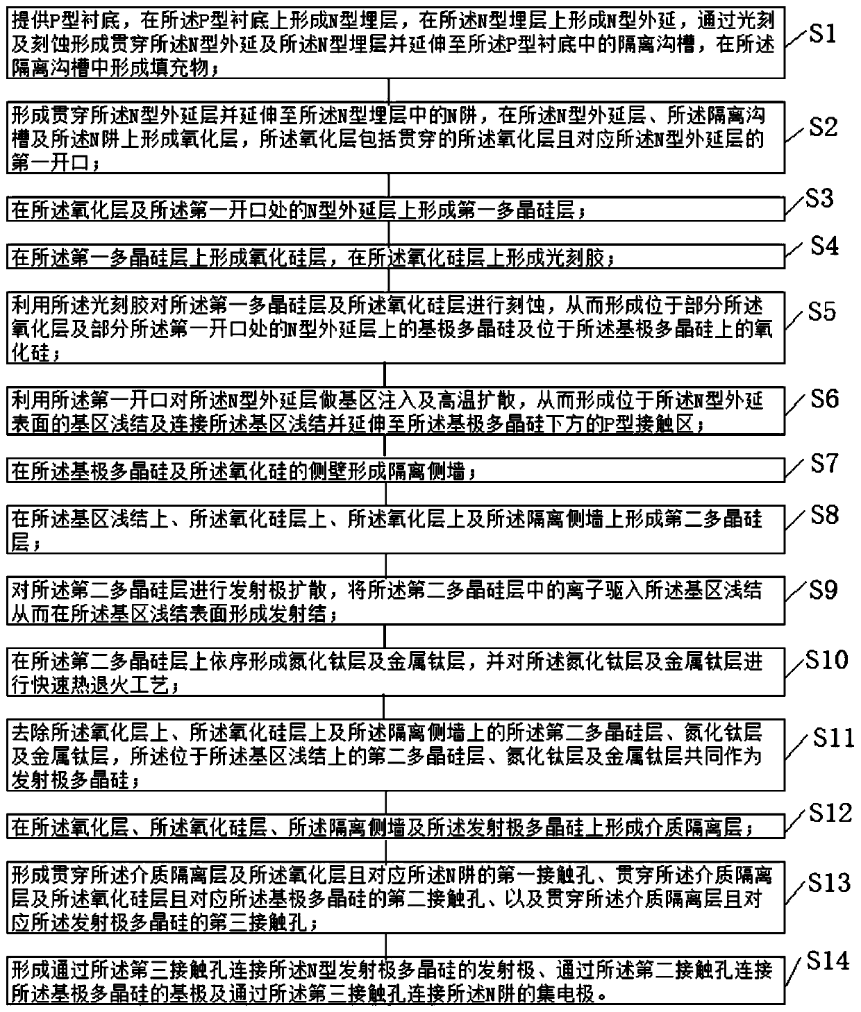
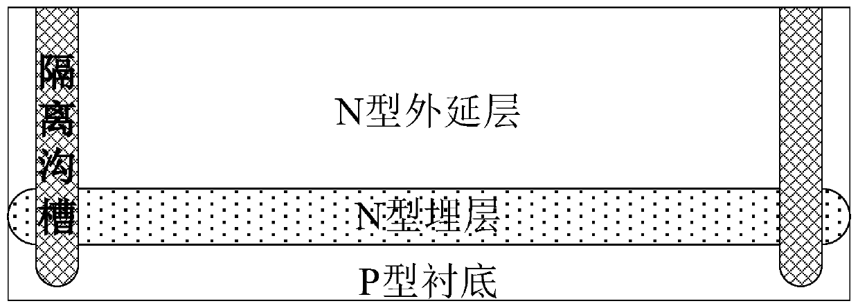
[0035] see Figure 1-Figure 12 , figure 1 It is a flow chart of the manufacturing method of the bipolar transistor of the present invention, Figure 2-Figure 12 for figure 1 The structural schematic diagram of each step of the manufacturing method of the bipolar transistor is shown. The manufacturing method of the bipolar transistor includes the following steps.

[0036] Step S1, see figure 2 , providing a P-type substrate, forming an N-type buried layer on the P-type substrate, forming an N-type epitaxial laye...


PUM

PropertyMeasurementUnit
thicknessaaaaaaaaaa
thicknessaaaaaaaaaa
thicknessaaaaaaaaaa

Abstract

The invention relates to a bipolar transistor and a manufacturing method thereof. During formation of an emitter polycrystalline silicon, the manufacturing method comprises the following steps: forming second polycrystalline silicon layers on base region shallow junctions, on a silicon oxide layer, on an oxide layer and on an isolating side wall; forming an emitter junction on the surface of the base region shallow junction, forming a titanium nitride layer and a metal titanium layer on the second polycrystalline silicon layers, and performing rapid thermal annealing on the titanium nitride layer and the metal titanium layer; and removing the second polycrystalline silicon layers, the titanium nitride layer and the metal titanium layer on the oxide layer, the silicon oxide layer and the isolating side wall, wherein the second polycrystalline silicon layers as well as the titanium nitride layer and the metal titanium layer positioned on the base region shallow junction are taken as theemitter polycrystalline silicon. According to the method disclosed by the invention, the emitter polycrystalline silicon is formed in a manner of sequentially depositing the second polycrystalline silicon layers, the titanium nitride layer and the metal titanium layer, and the problem in the current process that base-emitter short circuit is caused due to too small size of the polycrystalline emitter is solved.

Description

【Technical field】 [0001] The invention relates to the technical field of semiconductor manufacturing technology, in particular to a bipolar transistor and a manufacturing method thereof. 【Background technique】 [0002] It originated from the point-contact transistor transistor invented in 1948, and developed into a junction transistor in the early 1950s, which is now called a bipolar transistor. There are two basic structures of bipolar transistors: PNP type and NPN type. In these three layers of semiconductors, the middle layer is called the base region, and the outer two layers are called the emitter region and the collector region. When a small amount of current is injected into the base region, a larger current will form between the emitter region and the collector region, which is the amplification effect of the transistor. In bipolar transistors, both electrons and holes conduct electricity. Compared with field effect transistors, bipolar transistors have slow switc...

Claims


Application Information

Patent Timeline
Patent Type & Authority Patents(China)
IPC IPC(8): H01L21/331H01L21/28H01L29/417H01L29/735
CPCH01L29/401H01L29/41708H01L29/6625H01L29/735
Inventor 李龙梅小杰张泽清吴建忠杨东
Owner 深圳市金誉半导体股份有限公司
Why Eureka
Try Eureka