LED epitaxial structure and preparation method thereof

A technology of epitaxial structure and epitaxial layer, which is applied in the direction of electrical components, circuits, semiconductor devices, etc., and can solve problems such as affecting LED brightness and weakening luminous efficiency

Inactive Publication Date: 2018-07-06
ENRAYTEK OPTOELECTRONICS
View PDF6 Cites 2 Cited by
  • Summary
  • Abstract
  • Description
  • Claims
  • Application Information

AI Technical Summary

Problems solved by technology

In the application of high-end high-power LEDs, LEDs need to work under high current, but the luminous efficiency of LEDs will decrease with the increase of current, which will affect the brightness of LEDs

Method used


Image

  • LED epitaxial structure and preparation method thereof
  • LED epitaxial structure and preparation method thereof
  • LED epitaxial structure and preparation method thereof

Examples


preparation example Construction

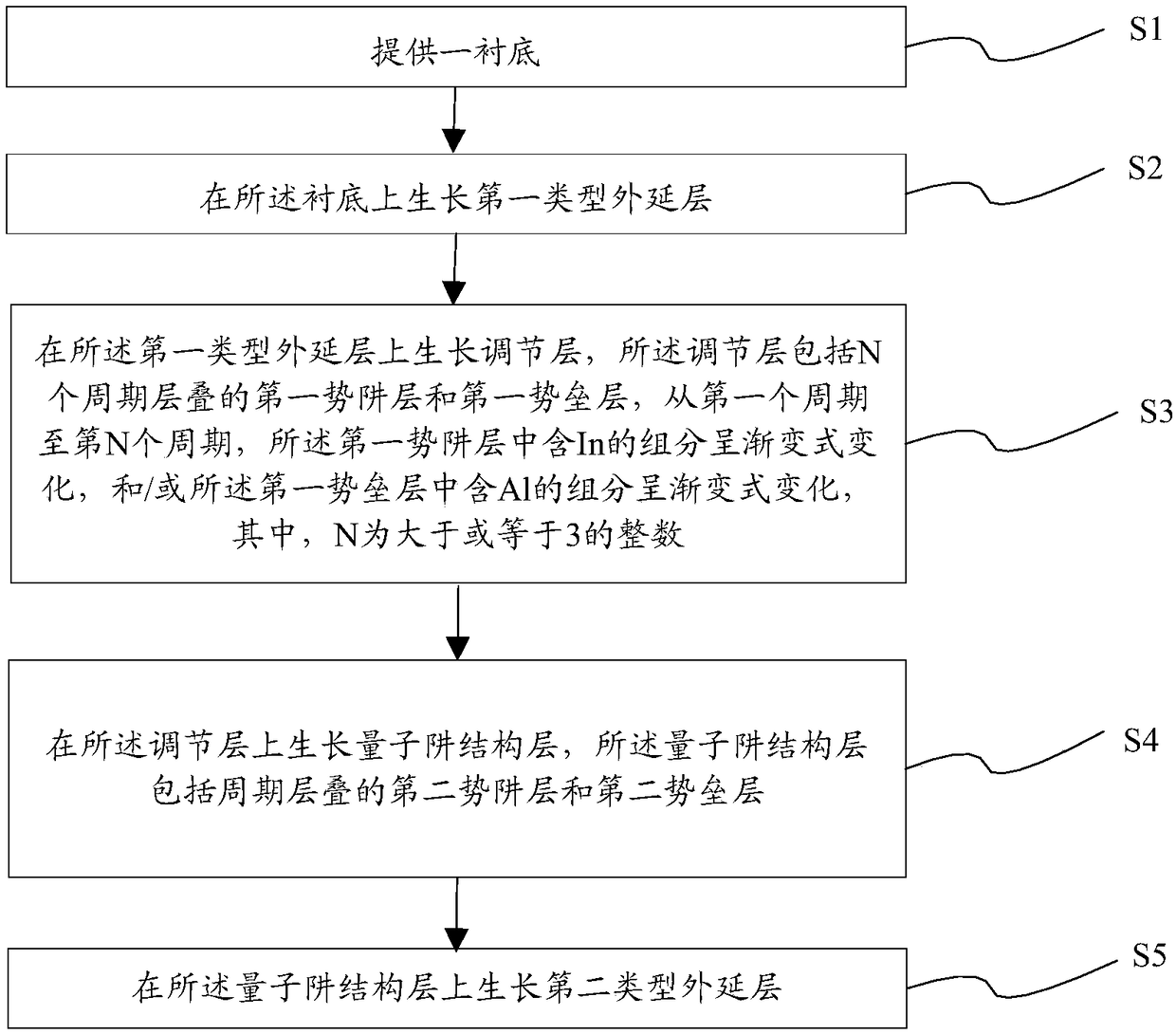
[0051] Correspondingly, the present invention also provides a method for preparing an LED epitaxial structure, such as figure 1 Shown: described preparation method comprises the following steps:

[0052] Step S1, providing a substrate;

[0053] Step S2, growing a first type epitaxial layer on the substrate;

[0054] Step S3, growing an adjustment layer on the first type epitaxial layer, the adjustment layer includes a first potential well layer and a first barrier layer stacked in N periods, from the first period to the Nth period, so The composition containing In in the first potential well layer changes gradually, and / or the composition containing Al in the first barrier layer changes gradually, wherein N is an integer greater than or equal to 3;

[0055] Step S4, growing a quantum well structure layer on the adjustment layer, the quantum well structure layer including a second potential well layer and a second potential barrier layer stacked periodically;

[0056] Step S...

Embodiment 1

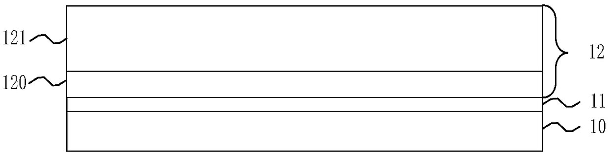
[0060] see figure 1 , firstly, step S1 is performed to provide a substrate 10, such as figure 2 shown. The substrate 10 may be a sapphire substrate, a gallium nitride substrate, an aluminum nitride substrate, a silicon substrate or a silicon carbide substrate, etc. The substrate 10 in this embodiment is preferably a sapphire substrate.

[0061] Then, if figure 1 As shown, step S2 is performed to grow the first type epitaxial layer 12 on the substrate 10, such as image 3 shown. The epitaxial growth method can be MOCVD (metal organic chemical vapor deposition) method, CVD (chemical vapor deposition) method, PECVD (plasma enhanced chemical vapor deposition) method, MBE (molecular beam epitaxy) method or HVPE (hydride vapor phase epitaxy) method etc. In this embodiment, the epitaxial growth method may preferably be the MOCVD method, which is not limited here. In the actual epitaxial growth process, in order to improve the crystal quality of LED epitaxial growth, a nucleatio...

Embodiment 2

[0071] see Figure 7 , where with Figure 2-Figure 6 The same reference numerals denote the same structures as those of the first embodiment. The preparation method of the second embodiment is basically the same as the preparation method of the first embodiment, the difference is that in step S3, as Figure 7 As shown, the adjustment layer 13' includes N periodic stacked first potential well layers and first barrier layers, N is an integer greater than or equal to 3, and the growth temperature of the adjustment layer 13' can be controlled at 700 degrees Celsius to Between 900 degrees Celsius, such as 800 degrees Celsius or 850 degrees Celsius; the thickness of the first potential well layer is 1.0 nm to 3.0 nm, and the thickness of the first barrier layer is 2.0 nm to 4.0 nm. The first potential well layer is In x Ga 1-x N, the first barrier layer is Al y Ga 1-y N, wherein the composition x of In is between 0% and 25%, and the composition y of Al is between 0% and 40%. ...


PUM


Abstract

The invention discloses an LED epitaxial structure and a preparation method thereof. The LED epitaxial structure comprises a substrate, a first type expitaxial layer located on the substrate, and an adjusting layer located on the first type expitaxial layer, a quantum well structure layer located on the adjusting layer and a second type epitaxial layer located on the quantum well structure layer,wherein the adjusting layer comprises a first potential well layer and a first potential barrier layer which are stacked by N periods, from the first period to the N period, components containing In in the first potential well layer taperingly change, and/or components containing A1 in the first potential barrier layer taperingly change, N is an integer larger than or equal to three; the adjustinglayer is added between the first type epitaxial layer and the quantum well structure layer, the components containing In of the first potential well layer in the adjusting layer and/or the componentscontaining A1 of the first potential barrier layer in the adjusting layer taperingly change, thereby improving the crystalline quality and the stress state of the epitaxial layer, effectively improving the problem of current carrier leakage under large current, and improving the LED luminance.

Description

technical field [0001] The invention belongs to the field of semiconductor light emitting, in particular to an LED epitaxial structure and a preparation method thereof. Background technique [0002] With the advancement of science and technology and the development of new energy sources, light emitting diodes (Light Emitting Diode, referred to as LED) are more and more widely used, such as high-end high-power high-brightness LED applications such as commercial lighting, stage lights, car headlights or pocket projectors. In the application of high-end high-power LEDs, LEDs need to work under high currents, but the luminous efficiency of LEDs will decrease with the increase of current, which will affect the brightness of LEDs. [0003] Therefore, in order to solve the above problems, it is necessary to provide an LED epitaxial structure and a preparation method thereof to improve the brightness of the LED under high current. Contents of the invention [0004] The invention ...

Claims


Application Information

Patent Timeline
Patent Type & Authority Applications(China)
IPC IPC(8): H01L33/02H01L33/00
Inventor 卢国军马后永
Owner ENRAYTEK OPTOELECTRONICS
Why Eureka
Try Eureka