Metamaterial manufacturing method
A manufacturing method and metamaterial technology, applied in the field of metamaterials, can solve the problems of low processing accuracy, high cost, poor implementability, etc., and achieve the effects of good electromagnetic corresponding characteristics, high manufacturing efficiency, and strong implementability.
- Summary
- Abstract
- Description
- Claims
- Application Information
AI Technical Summary
Problems solved by technology
Method used
Image

Examples
Embodiment 1
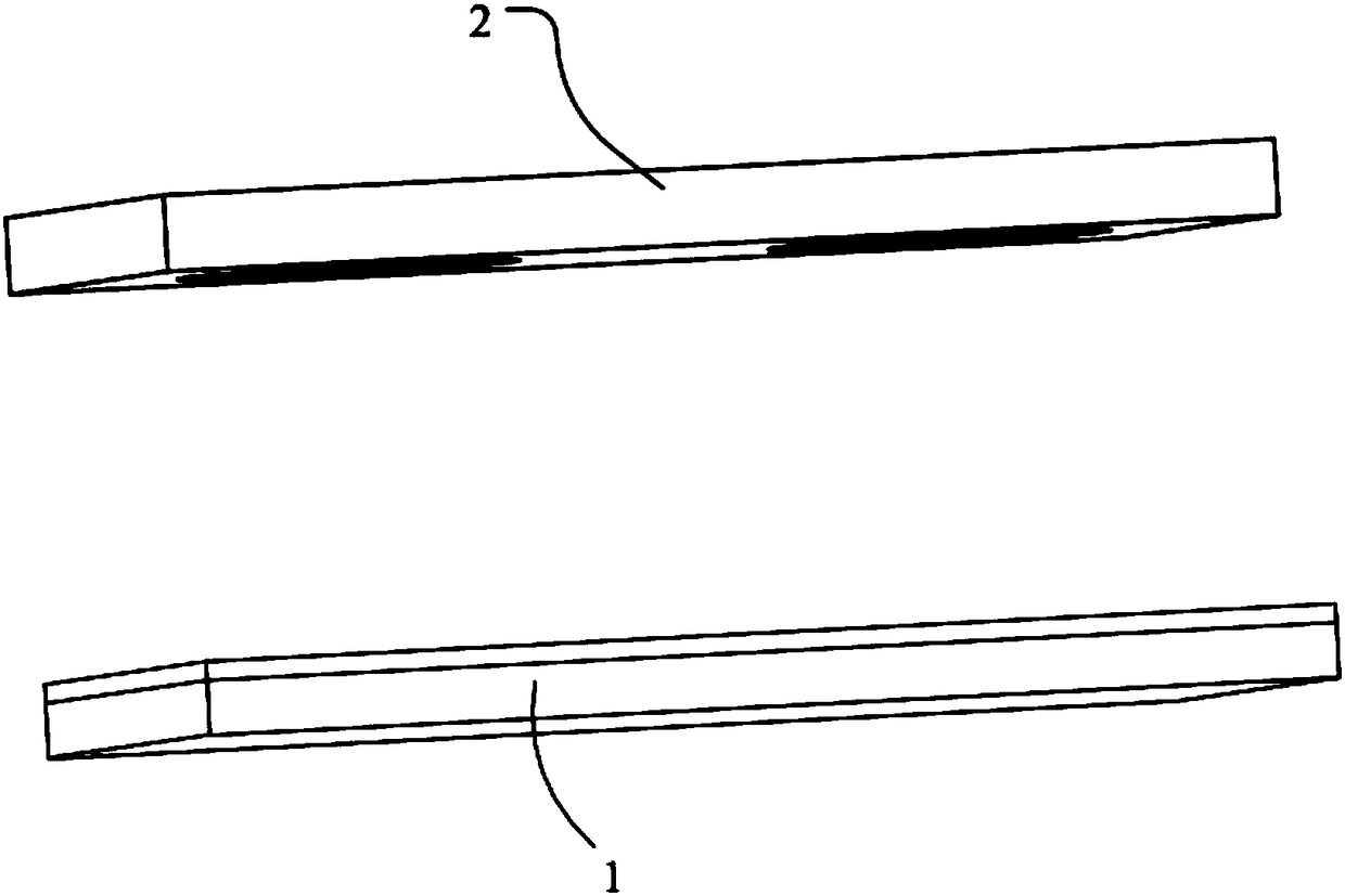
[0043] In step S01, see figure 1 , to prepare the soft template 2 with the reverse pattern of the microstructure of the metamaterial 1.
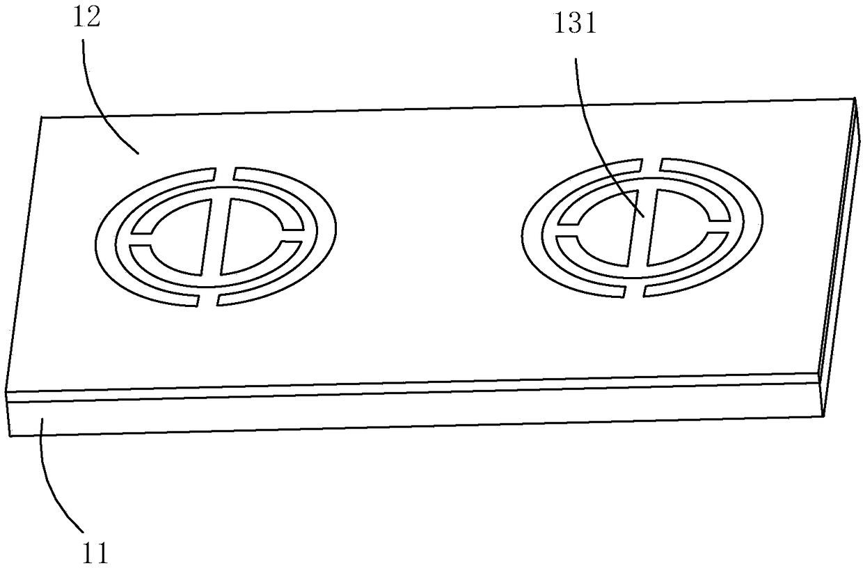
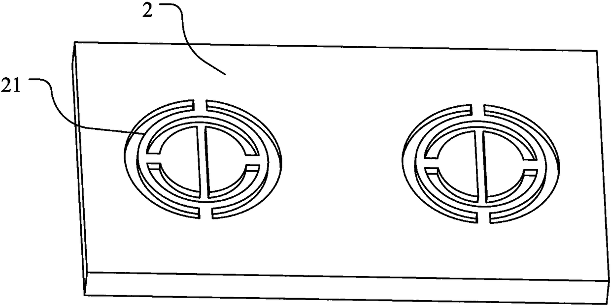
[0044] Specifically, the soft template 2 is a PDMS template, which is made of PDMS, that is, polydimethylsiloxane material, which has good flexibility and low surface energy, so that its surface is opposite to, for example, octadecane Materials such as trichlorosilane (OTS) have less adhesion. The preparation of the soft template 2 can adopt a photolithography method to form a pattern opposite to the microstructure on the surface of a hard substrate. Resist, wherein the part corresponding to the microstructure is left blank, while the other part is set as photoresist. like image 3 As shown, the pattern formed on the surface of the hard substrate is a plurality of split ring-shaped grooves 21 defined by photoresist that match the shape and size of the split resonant ring 131 . After the hard substrate with the patterned photoresist is ob...
Embodiment 2
[0061] In step S01, a soft template 2 having a pattern opposite to the microstructure of the metamaterial 1 is prepared.
[0062] Specifically, the soft template 2 is a PDMS template, which is made of PDMS, that is, polydimethylsiloxane material, which has good flexibility and low surface energy, so that its surface is opposite to, for example, octadecane Materials such as trichlorosilane (OTS) have less adhesion. The preparation of the soft template 2 can adopt a photolithography method to form a pattern opposite to the microstructure on the surface of a hard substrate. The pattern opposite to the microstructure in this embodiment refers to setting patterned light on the surface of the hard substrate Resist, wherein the part corresponding to the microstructure is left blank, and the other part is set as photoresist. In this embodiment, the pattern formed on the surface of the hard substrate is matched with the shape and size of the split resonator ring 131 A plurality of ope...
Embodiment 3
[0079] In step S01, a soft template 2 having a pattern opposite to the microstructure of the metamaterial 1 is prepared.
[0080] Specifically, the soft template 2 is a PDMS template, which is made of PDMS, that is, polydimethylsiloxane material, which has good flexibility and low surface energy, so that its surface is opposite to, for example, octadecane Materials such as trichlorosilane (OTS) have less adhesion. The preparation of the soft template 2 can adopt a photolithography method to form a pattern opposite to the microstructure on the surface of a hard substrate. The pattern opposite to the microstructure in this embodiment refers to setting patterned light on the surface of the hard substrate Resist, in which the part corresponding to the microstructure is left blank, while the other part is set as photoresist such as image 3 As shown, the pattern processed on the surface of the hard substrate is a plurality of split ring-shaped grooves 21 defined by photoresist tha...
PUM
 Abstract
Description
Claims
Application Information