
A kind of bipolar bistable memristor and preparation method thereof

A memristor and bistable technology, which is applied in the field of micro-nano electronic devices, can solve the problems of slow response speed, poor stability, and low memory cell density of memristors, so as to reduce power consumption, improve stability, and avoid unevenness. uneven effect

Active Publication Date: 2019-09-03
CENT SOUTH UNIV
View PDF12 Cites 0 Cited by
  • Summary
  • Abstract
  • Description
  • Claims
  • Application Information

AI Technical Summary

Problems solved by technology

For example, the patent CN102738387A discloses a memristor based on a single-layer TiOx (0.5<x<3) film structure and its preparation method, and obtains a memristor with a resistive layer composed of a single-layer TiOx film, which is effective Reduces the production cost of memristors, but its memristor memory cells have low density, slow response speed, and poor stability

Method used


Image

  • A kind of bipolar bistable memristor and preparation method thereof
  • A kind of bipolar bistable memristor and preparation method thereof
  • A kind of bipolar bistable memristor and preparation method thereof

Examples


Embodiment 1

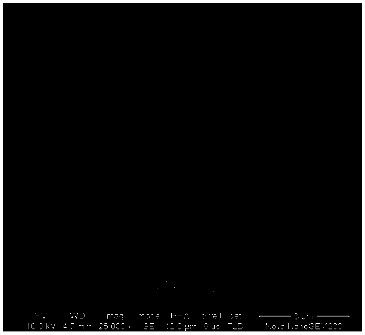
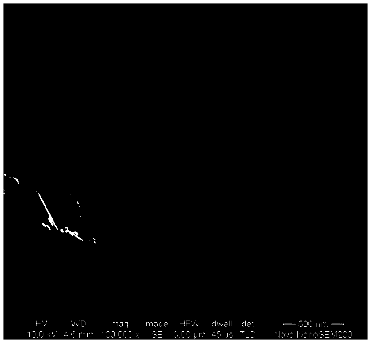
[0021] The surface of the FTO conductive glass is ultrasonically cleaned with acetone and alcohol successively to obtain the FTO conductive glass bottom electrode. The acid solution of tetrabutyl titanate (the acid solution is a hydrochloric acid aqueous solution with a mass fraction of 50%) is prepared according to the titanium element concentration of 0.07 mol / L. Will be 4cm 2 FTO conductive glass is placed in an autoclave, and then 0.238ml of acid solution of tetrabutyl titanate is added. After the device is compressed, it is placed in a blast drying oven and heated at 130°C for 4 hours. After the reaction is completed, take out the sample The parts are cleaned with pure water to neutrality to obtain FTO conductive glass on which titanium dioxide nanowire arrays are grown on the surface. Its microscopic appearance is like figure 1 As shown, it can be seen from the figure that a layer of titanium dioxide nanowire arrays are grown on FTO conductive glass. The nanowire arrays a...

Embodiment 2

[0027] The surface of the FTO conductive glass is ultrasonically cleaned with acetone and alcohol successively to obtain the FTO conductive glass bottom electrode. An acid solution of tetrabutyl titanate (the acid solution is a hydrochloric acid aqueous solution with a mass fraction of 50%) is prepared according to the titanium element concentration of 0.03 mol / L. Will be 4cm 2 FTO conductive glass is placed in an autoclave, and then 0.1ml of acid solution of tetrabutyl titanate is added. After pressing the device, it is placed in a blast drying oven and heated at 200°C for 1 hour. After the reaction is completed, take out the sample The parts are cleaned with pure water to neutrality to obtain FTO conductive glass on which titanium dioxide nanowire arrays are grown on the surface. The average length of the obtained titanium dioxide nanowires was 1 um, and the average diameter of the nanowires was 100 nm.

[0028] Then a layer of titanium dioxide film is suspended on the titaniu...

Embodiment 3

[0032] The surface of the FTO conductive glass is ultrasonically cleaned with acetone and alcohol successively to obtain the FTO conductive glass bottom electrode. An acid solution of tetrabutyl titanate (the acid solution is an aqueous hydrochloric acid solution with a mass fraction of 50%) is prepared according to the titanium element concentration of 0.1 mol / L. Will be 4cm 2 FTO conductive glass is placed in the autoclave, and then 0.340ml of acid solution of tetrabutyl titanate is added. After the device is compressed, it is placed in a blast drying box and heated at 80°C for 48 hours. After the reaction is completed, take out the sample The parts are cleaned with pure water to neutrality to obtain FTO conductive glass on which titanium dioxide nanowire arrays are grown on the surface. The average length of the obtained titanium dioxide nanowires is 6um, and the average diameter of the nanowires is 200nm.

[0033] Then, a layer of titanium dioxide film was suspended on the t...


PUM

PropertyMeasurementUnit
lengthaaaaaaaaaa
diameteraaaaaaaaaa
thicknessaaaaaaaaaa

Abstract

The object of the present invention is to disclose a bipolar bistable memristor, which includes an upper electrode, a lower electrode, and a resistance transition layer between the two electrodes. The resistance transition layer is composed of a titanium dioxide nanowire array and coated on TiO2 film on nanowire arrays. The resistance transition layer of the present invention is composed of titanium dioxide nanowires and titanium dioxide thin films. Titanium dioxide nanowires have high density characteristics and are prepared into memristors, which can realize high-density storage of memristors, improve the response speed of memristors, and reduce The power consumption of the memristor; coating a layer of titanium dioxide film on the titanium dioxide nanowire can avoid the leakage current caused by the uneven nanowire and insufficient contact with the metal upper electrode, thereby improving the stability of the memristor.

Description

Technical field [0001] The invention belongs to the technical field of micro-nano electronic devices, and specifically relates to a bipolar bistable memristor and a preparation method thereof. Background technique [0002] The memristor is a basic circuit element, the resistance of the device can produce a non-linear response to the stimulation of magnetic flux or input voltage and can be maintained. The principle of the memristor was first proposed by Professor Shaotang Tsai of the University of California, Berkeley. Until 2008, researchers at HP Labs obtained the world’s first working memristor prototype, thus confirming the memristor theory. Aroused people's great interest, and conducted a lot of mechanism research and applied research. In recent years, in order to achieve greater integration, the preparation of small-sized memristor devices is an inevitable trend in the development of memristors. If memristors can be realized, they can be structured at the nanometer level. T...

Claims


Application Information

Patent Timeline
Patent Type & Authority Patents(China)
IPC IPC(8): H01L45/00
CPCH10N70/883H10N70/026
Inventor 姜超余延涛黄小忠王春齐岳建岭杜作娟蒋礼
Owner CENT SOUTH UNIV
Learn More