Improved electrochromic device
An electrochromic device, conductivity technology, applied in instruments, nonlinear optics, optics, etc., can solve the problems of influence effect, poor solubility, increase the viscosity of electrochromic solution, etc., to reduce defects, high reflection area Effect
- Summary
- Abstract
- Description
- Claims
- Application Information
AI Technical Summary
Problems solved by technology
Method used
Image
Examples
Embodiment 1
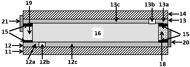
[0072] by 10 wt%SnO 2 and 90 wt%In 2 o 3 The sintered ceramics are used as the target material, and the radio frequency magnetron sputtering method (room temperature, oxygen and argon mixed atmosphere, sputtering pressure is 0.5Pa, oxygen partial pressure is 1×10 -2 Pa, power 100W, time 30min) deposit a layer of indium tin oxide conductive layer with a thickness of 150 nm on the first glass substrate, and use a conductive sealant (Threebond THREEBOND3301F halogen-free anisotropic conductive silver sealant from Japan) to A metal copper sheet with a width of 15 mm and a thickness of 380 μm is bonded to the edge of the indium tin oxide transparent conductive layer, and its front end is 4 mm from the edge.
[0073] by (1-x)ZnO+xAl 2 o 3 (x = 2 wt%) sintered ceramics as the target (the target is doped with Al 2 o 3 A ceramic target made of powdered ZnO powder sintered at high temperature, Al in ZnO powder 2 o 3 The mass fraction is 2%, ), by radio frequency magnetron sputte...
Embodiment 2
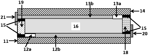
[0077] by 10 wt%SnO 2 and 90 wt%In 2 o 3 The sintered ceramics were used as the target material, and a transparent conductive layer of indium tin oxide with a thickness of 150 nm was deposited on the first glass substrate by radio frequency magnetron sputtering (the sputtering process was the same as that in Example 1). Tiantian HT6307 type) bond a metal stainless steel iron sheet with a width of 12 mm and a thickness of 550 μm on the transparent conductive layer of indium tin oxide, and its front end is 5 mm away from the edge.
[0078] by (1-x)ZnO+xAl 2 o 3 (x = 2 wt%) sintered ceramics are used as the target, and a layer of aluminum-doped zinc oxide transparent with a thickness of 150 nm is deposited on the second glass substrate by radio frequency magnetron sputtering (the sputtering process is the same as in Example 1). For the conductive layer, another metal copper sheet with a width of 12 mm and a thickness of 550 μm is also bonded to the transparent conductive laye...
Embodiment 3
[0082] by 10 wt%SnO 2 and 90 wt%In 2 o 3 The sintered ceramics were used as the target material, and a conductive layer of indium tin oxide with a thickness of 150 nm was deposited on the first glass substrate by radio frequency magnetron sputtering (the sputtering process was the same as in Example 1), and a conductive sealant ( Shenzhen Huatianhe Technology Co., Ltd. TH-3001 type) bond a metal aluminum sheet with a width of 15 mm and a thickness of 300 μm on the indium tin oxide conductive layer, and its front end is 3 mm away from the edge.
[0083] Using metal silver as the target material, through radio frequency magnetron sputtering (silver target, the purity is 99.99%; the sputtering condition is: the background vacuum is 1×10 -3 Pa, the working pressure is 0.3Pa, the power is 16W, and the time is 5 min) to deposit a silver layer with a thickness of 10 nm on the second glass substrate; by 10 wt% SnO 2 and 90 wt%In 2 o 3 The sintered ceramic was used as the target m...
PUM
| Property | Measurement | Unit |
|---|---|---|
| thickness | aaaaa | aaaaa |
| thickness | aaaaa | aaaaa |
| width | aaaaa | aaaaa |
Abstract
Description
Claims
Application Information


