

Preparation method of high-luminance V-shaped polarized doped deep ultraviolet LED
A polarized doping and high-brightness technology, which is applied to electrical components, circuits, semiconductor devices, etc., can solve the problems of reduced light extraction efficiency of LED devices
- Summary
- Abstract
- Description
- Claims
- Application Information
AI Technical Summary
Problems solved by technology
Method used
Image

Examples
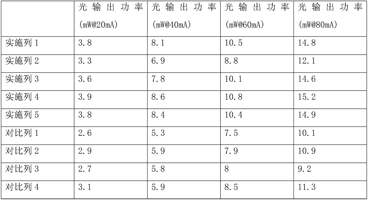
Embodiment 1
[0034] S1. On the sapphire substrate, first grow an aluminum nitride (AlN) buffer layer with a thickness of 25nm at low temperature. The / III molar ratio is 5000-5500, and the growth thickness is 25 nanometers.
[0035] S2. Growing a high-temperature aluminum nitride (AlN) buffer layer with a thickness of 500 nm on the low-temperature aluminum nitride (AlN) buffer layer. Growth conditions: the growth temperature is 1050°C, the reaction chamber pressure is 40torr, the ammonia gas flow rate is 8000μmol / min, and the V / III molar ratio is 5000.
[0036] S3. Growing a 1.5-micron-thick N-type AlGaN stress release layer with a composition gradient on the high-temperature aluminum nitride (AlN) buffer layer. Growth conditions: growth temperature is 1050°C, reaction chamber pressure is 40torr, TMGa flow rate is 17μmol / min, TMAl flow rate is 2-5.5μmol / min, SiH 4 The flow rate is 7-9 nmol / min, the flow rate of ammonia gas is 10000 μmol / min, and the growth thickness is 1.5 μm.
[0037] ...
Embodiment 2
[0042] S1. On the composite substrate of sapphire and aluminum nitride (Al 2 o 3 / AlN), first grow an aluminum nitride (AlN) buffer layer with a thickness of 15nm at low temperature, the growth conditions: the growth temperature is 650°C, the reaction chamber pressure is 50torr, the ammonia flow rate is 9000μmol / min, and the V / III molar ratio is 5000~5500.
[0043] S2. Growing a high-temperature aluminum nitride (AlN) buffer layer with a thickness of 300 nm on the low-temperature aluminum nitride (AlN) buffer layer. Growth conditions: the growth temperature is 1080°C, the reaction chamber pressure is 50torr, the ammonia gas flow rate is 9000μmol / min, and the V / III molar ratio is 5500.
[0044] S3. Growing an N-type AlGaN stress release layer with a thickness of 1 micron on the high-temperature aluminum nitride (AlN) buffer layer. Growth conditions: growth temperature is 1080°C, reaction chamber pressure is 50torr, TMGa flow rate is 17μmol / min, TMAl flow rate is 2-5.5μmol / mi...
Embodiment 3
[0049] Steps S1 to S5 are the same as in Embodiment 1.
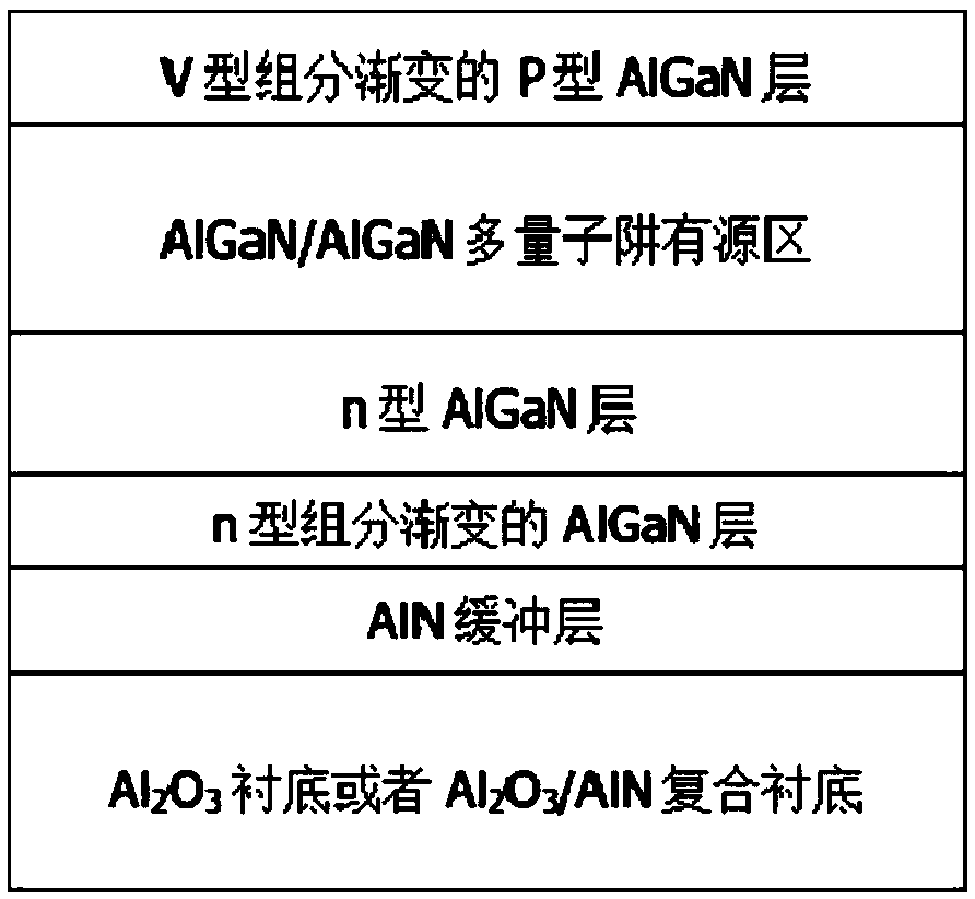
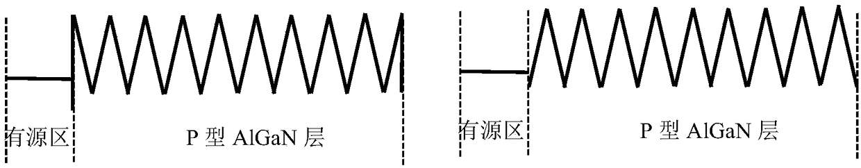
[0050] S6. On the deep ultraviolet light-emitting layer, grow a V-shaped P-type AlGaN layer with a total thickness of 110 nm, each V-shaped layer has a thickness of 12.22 nm, and the others are the same as in Example 1.
PUM
| Property | Measurement | Unit |
|---|---|---|
| Thickness | aaaaa | aaaaa |
| Thickness | aaaaa | aaaaa |
| Thickness | aaaaa | aaaaa |
Abstract
Description
Claims
Application Information