Unlock instant, AI-driven research and patent intelligence for your innovation.

Preparation method of source field plate of GaN-based HEMT device and HEMT device

A source field plate and device technology, applied in semiconductor/solid-state device manufacturing, semiconductor devices, electrical components, etc., can solve the problem that the performance of GaN-based HEMT devices cannot be well improved, and achieve the effect of improving performance

Active Publication Date: 2018-08-10
THE 13TH RES INST OF CHINA ELECTRONICS TECH GRP CORP
View PDF4 Cites 1 Cited by
  • Summary
  • Abstract
  • Description
  • Claims
  • Application Information

AI Technical Summary

Problems solved by technology

[0004] In view of this, an embodiment of the present invention provides a method for preparing a source field plate of a GaN-based HEMT device and a HEMT device, so as to solve the problem that the source field plate structure in the prior art cannot well improve the performance of a GaN-based HEMT device

Method used


Image

  • Preparation method of source field plate of GaN-based HEMT device and HEMT device
  • Preparation method of source field plate of GaN-based HEMT device and HEMT device
  • Preparation method of source field plate of GaN-based HEMT device and HEMT device

Examples


Embodiment 1

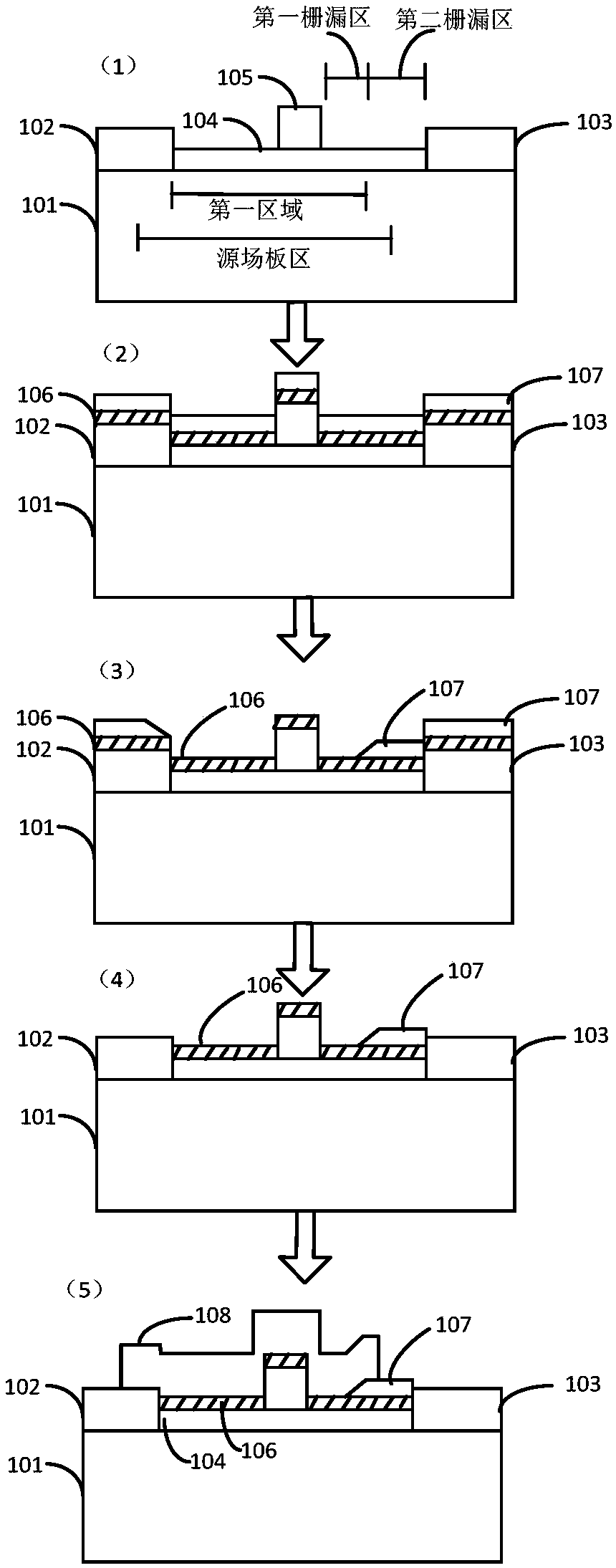
[0040] Please refer to figure 2 , a method for preparing a source field plate of a GaN-based HEMT device, comprising:

[0041] Step S201, sequentially growing a SiN layer of the first thickness and a SiO layer of the second thickness on the upper surface of the device 2 layer.

[0042] In the embodiment of the present invention, please refer to figure 1 (2), first clean the GaN-based HEMT device, and then sequentially deposit a SiN layer 106 with a first thickness and a SiO with a second thickness on the upper surface of the device by an ion-enhanced chemical vapor deposition (Plasma Enhanced Chemical Vapor Deposition, PECVD) process 2 layer 107, SiN layer 106 and SiO 2 Layer 107 serves as two dielectric layers with high etch selectivity. SiN layer 106 and SiO 2 The thickness of layer 107 can be set according to actual needs, preferably, the thickness of SiN layer 106 is 50 nanometers to 200 nanometers, SiO 2 Layer 107 has a thickness of 50 nm to 800 nm.

[0043] Step ...

Embodiment 2

[0058] Please refer to Figure 5 , a HEMT device, comprising a HEMT device body, a source gate region, a gate electrode region and a gate drain region of the HEMT device body covering a SiN layer 106 of a first thickness, the SiN layer 106 corresponding to the first gate drain region The upper surface is covered with a second thickness of SiO 2 layer 107, the SiO 2 The surface of layer 107 facing the gate electrode region is inclined; wherein, the first gate drain region is connected to the drain electrode region; the source field plate region on the upper surface of the HEMT device covers the metal layer 108 with a third thickness , the source field plate region includes a preset portion of the source electrode region, a source gate region, a gate electrode region and a preset portion of the gate drain region, the preset portion of the source electrode region, the source gate region, the gate The predetermined parts of the electrode region and the gate-drain region are sequ...


PUM

PropertyMeasurementUnit
Thicknessaaaaaaaaaa
Thicknessaaaaaaaaaa
Thicknessaaaaaaaaaa

Abstract

The invention provides a preparation method of a source field plate of a GaN-based HEMT device and the HEMT device suitable for the technical field of semiconductors. The method comprises that a SiN layer in a first thickness and a SiO2 layer in a second thickness are grown in the upper surface of the device successively; a part corresponding to a first area is removed from the SiO2 layer; the surface, toward a gate electrode region, of a part, corresponding to a second gate-drain area, in the residual area of the SiO2 layer is an inclined surface with a first inclination angle; parts corresponding to the source and drain electrode regions are removed from the SiO2 layer as well as the SiN layer successively; a metal layer in a third thickness is grown in a part, corresponding to a sourcefield plate area, in the upper surface of the device; and the metal layer covers the inclined surface of the part, corresponding to the second gate-drain area, of the SiO2 layer. The field plate prepared by the method is of a wedge-shaped structure, a die breakdown voltage can be improved substantially, a circuit avalanche effect can be inhibited, and performance of the device is improved substantially.

Description

technical field [0001] The invention belongs to the technical field of semiconductors, and in particular relates to a preparation method of a GaN-based HEMT device source field plate and a HEMT device. Background technique [0002] Due to the advantages of high breakdown voltage, high power density, high electron mobility, and high electron saturation drift velocity, GaN devices have broad application prospects in military and civilian fields such as radar, aerospace, communications, and power electronics. [0003] GaN-based high electron mobility transistor (High Electron Mobility Transistor, HEMT) is a commonly used semiconductor device. During the working process of GaN-based HEMT devices, the drain terminal voltage can be as high as 50V or more, while the gate terminal voltage is generally -5V~5V, so the drain terminal gate edge electric field can be as high as MV / cm when the device is working. Because the GaN material has a very significant inverse piezoelectric effect...

Claims


Application Information

Patent Timeline
IPC IPC(8): H01L21/28H01L21/335H01L29/40H01L29/778
CPCH01L29/401H01L29/402H01L29/66462H01L29/778
Inventor 默江辉王川宝苏延芬崔雍宋洁晶崔玉兴
Owner THE 13TH RES INST OF CHINA ELECTRONICS TECH GRP CORP
Features
  • R&D
  • Intellectual Property
  • Life Sciences
  • Materials
  • Tech Scout
  • Unparalleled Data Quality
  • Higher Quality Content
  • 60% Fewer Hallucinations
Learn More