Method for integrating three-dimensional conductive metal micro-nano structure inside transparent material

A transparent material and micro-nano structure technology, applied in the direction of microstructure technology, microstructure devices, manufacturing microstructure devices, etc., can solve the problems of limited precision, inflexible geometric configuration of metal structure space, etc., and achieve high device stability Effect

Inactive Publication Date: 2018-08-14
EAST CHINA NORMAL UNIVERSITY
View PDF11 Cites 4 Cited by
  • Summary
  • Abstract
  • Description
  • Claims
  • Application Information

AI Technical Summary

Problems solved by technology

[0003] The technical problem to be solved by the present invention is to overcome the disadvantages of the existing three-dimensional conductive metal micro-nano structure integrated in the transparent material, such as the use stability of the metal micro-nano structure, inflexible

Method used


Image

  • Method for integrating three-dimensional conductive metal micro-nano structure inside transparent material
  • Method for integrating three-dimensional conductive metal micro-nano structure inside transparent material

Examples


Embodiment Construction

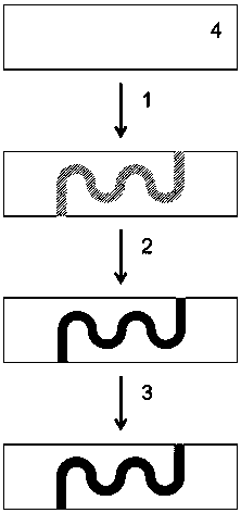
[0025] The present invention will be further described below in conjunction with the embodiments and accompanying drawings, but the protection scope of the present invention should not be limited thereby. figure 1 It is a schematic flow chart of integrating a three-dimensional metal micro-nano structure inside a transparent material in the present invention. Now take quartz glass as an example to illustrate the present invention. It can be seen from the figure that the present invention uses a femtosecond laser to integrate a three-dimensional conductive metal micro-nano structure in glass. The method includes the following steps:

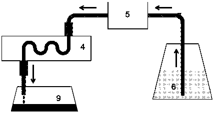
[0026] (1) Femtosecond laser irradiation: take a clean quartz glass sample 4 with a size of 10 mm×10 mm×2 mm and polish the upper and lower surfaces, and fix it on a three-dimensional translation stage; the femtosecond laser directly writes microchannels inside the quartz glass sample When patterning, the central wavelength is 515 nm, the repetitio...


PUM


Abstract

The invention discloses a method for integrating a three-dimensional conductive metal micro-nano structure inside a transparent material. The method comprises the following steps: firstly, preparing athree-dimensional micro-channel inside the transparent material by using the femtosecond laser micro-machining technology; and then continuously transmitting electroless plating solution through a peristaltic pump, carrying out surface modification and metal deposition inside the channel through the micro-channel, so that the three-dimensional conductive metal micro-nano structure is integrated inside the transparent material. According to the integrated three-dimensional conductive metal micro-nano structure manufactured by the invention, the space shape can be randomly designed, the size isadjustable, the electrical conductivity is high, and the melting point is high; and the integrated three-dimensional conductive metal micro-nano structure has great application prospect in the technical fields of microelectronic devices, optoelectronic devices, micro-nano motor systems and the like.

Description

technical field [0001] The invention relates to three-dimensional metal structure manufacturing and femtosecond laser micromachining, in particular to a method for integrating a three-dimensional conductive metal micro-nano structure in a transparent material by combining femtosecond laser micromachining and flow chemical plating. The invention is suitable for integrating a three-dimensional conductive metal micro-nano structure inside various transparent materials such as glass, crystal and transparent polymer. Background technique [0002] The three-dimensional metal micro-nano structure integrates the characteristics of metal and three-dimensional micro-nano structure, and has shown great application potential in the fields of microelectronics, optoelectronics, biomedicine and so on. Based on the above characteristics, people are exploring the integration of three-dimensional metal micro-nano structures on the chip to enhance the functionality and active regulation capabi...

Claims


Application Information

Patent Timeline
IPC IPC(8): B81C1/00
CPCB81C1/00B81C1/00436
Inventor 程亚徐剑敬承斌钟熠李晓龙
Owner EAST CHINA NORMAL UNIVERSITY
Why Eureka
Try Eureka