Model for calculating channel potential and current of gallium nitride-based high-power high electron mobility transistor with high power

A high electron mobility, gallium nitride-based technology, applied in the field of models for calculating the channel potential and current of gallium nitride-based high electron mobility transistors, to achieve the effects of fast circuit simulation tools, concise form, and clear physical concepts

Active Publication Date: 2018-08-17
FUDAN UNIV
View PDF3 Cites 4 Cited by
  • Summary
  • Abstract
  • Description
  • Claims
  • Application Information

AI Technical Summary

Problems solved by technology

The traditional bulk device model is no longer suitable, which brings new challenges to the modeling and simulation of new material devices

Method used


Image

  • Model for calculating channel potential and current of gallium nitride-based high-power high electron mobility transistor with high power
  • Model for calculating channel potential and current of gallium nitride-based high-power high electron mobility transistor with high power
  • Model for calculating channel potential and current of gallium nitride-based high-power high electron mobility transistor with high power

Examples


Embodiment Construction

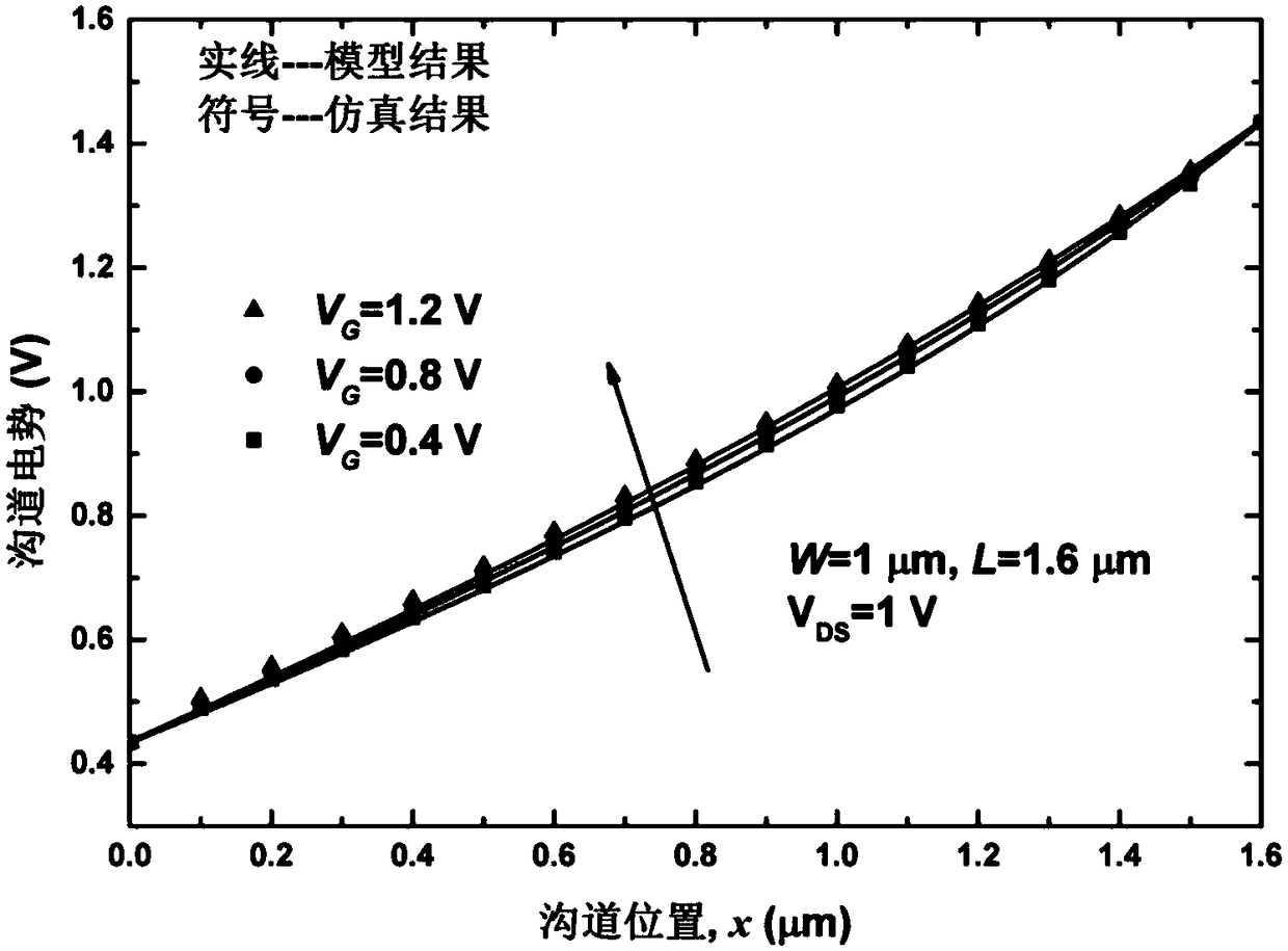
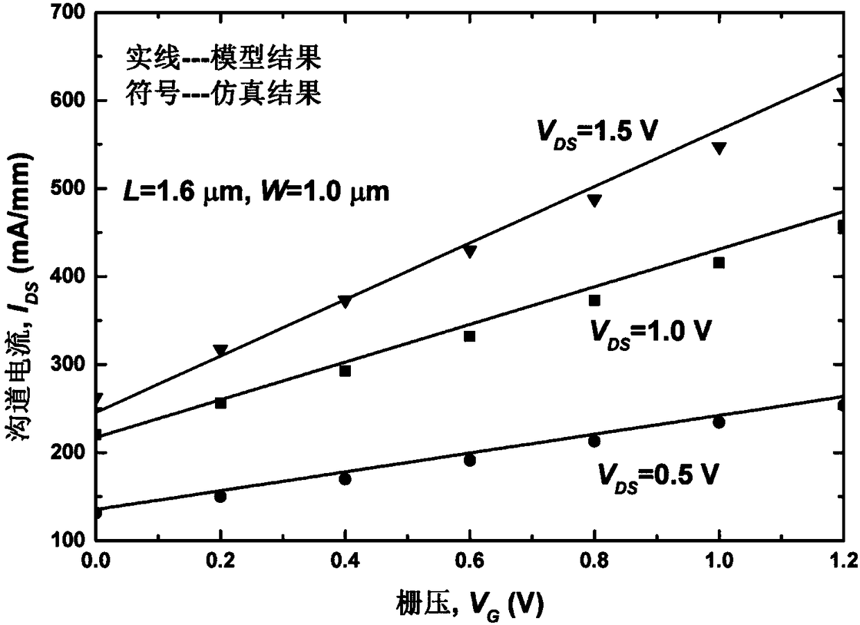
[0057] For GaN-based high-power HEMTs, our analytical model calculations and the results obtained using the Sentaurus 3D simulation software are in good agreement, such as figure 2 , 3 , 4 shown. In practical application, the present invention can adjust the fitting parameters λ, μ for different process conditions 0 , θ 1 , θ 2 and α to get the model calibrated. then according to Figure 5 The process can be very convenient to obtain relevant results, and the analytical expression can be embedded in the circuit simulation software.

[0058] Description of device parameters: Unless otherwise specified, the device parameters used in all simulations and models are: device width W=1μm, intrinsic AlGaN thickness of 5nm, doped AlGaN thickness of 25nm, V off =-1.95V,μ 0 =1600cm 2 / Vs, α=0.78, λ=10 -4 ,θ 1 =10 -3 , θ 2 =10 -5 .


PUM


Abstract

The invention belongs to the technical field of integrated circuit semiconductors, and specifically discloses a model for calculating channel potential and current of a gallium nitride-based high-power high electron mobility (HEMT) transistor with high power. The structure of the transistor is a heterojunction and the transistor is prepared through the following steps of: carrying out epitaxial growth on AlGaN on un-doped GaN through a molecular beam; carrying out n-type degenerate doping on the AlGaN; and arranging a layer of thin intrinsic AlGaN between the doped AlGaN and GaN so as to decrease scattering from donor atoms to electrons. The transistor can be used for high-power electrons. According to the model, channel potential and two-dimensional electron gas charge density of the transistor are solved, and drift and diffusion of electrons are considered, so that a relational expression between current at any channel and the potential is obtained; and compound and generated currentare neglected, and the current at different channel points is equal, so that an analytical expression between channel potential and source / drain current is obtained. The model has a concise form anda clear physical concept, and provides a rapid circuit simulation tool for circuit simulation software during the research of high-power HEMT devices.

Description

technical field [0001] The invention belongs to the technical field of integrated circuits and semiconductors, in particular to a model for calculating the channel potential and current of gallium nitride-based high electron mobility transistors. Background technique [0002] With the continuous improvement of integrated circuit chip integration and the continuous shrinking of device geometry, traditional silicon devices will reach their limit in the near future and will be replaced by other non-silicon devices. GaN-based high-power devices, due to their high breakdown voltage, high saturation velocity, high electron mobility, and high electron surface density, will soon be widely used in high-speed, high-voltage, and high-power circuits. [0003] In order to facilitate the practical application of such devices in integrated circuits, it is particularly important to create analytical models, and the extraction models of their channel potential and current are increasingly co...

Claims


Application Information

Patent Timeline
Patent Type & Authority Applications(China)
IPC IPC(8): G06F17/50
CPCG06F30/39
Inventor 胡光喜刘冉郑立荣
Owner FUDAN UNIV
Why Eureka
Try Eureka