Gallium nitride semiconductor device and manufacturing method thereof

A manufacturing method and semiconductor technology, applied in the direction of semiconductor devices, semiconductor/solid-state device manufacturing, electrical components, etc., can solve problems such as low breakdown voltage, achieve the effects of increasing breakdown voltage, improving performance, and improving relief

Active Publication Date: 2018-08-21
INNOSCIENCE (ZHUHAI) TECH CO LTD
View PDF5 Cites 2 Cited by
  • Summary
  • Abstract
  • Description
  • Claims
  • Application Information

AI Technical Summary

Problems solved by technology

However, the breakdown voltage of existing gallium nitride semiconductor devices is low

Method used


Image

  • Gallium nitride semiconductor device and manufacturing method thereof
  • Gallium nitride semiconductor device and manufacturing method thereof

Examples


Embodiment Construction

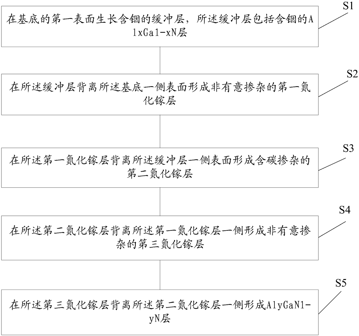
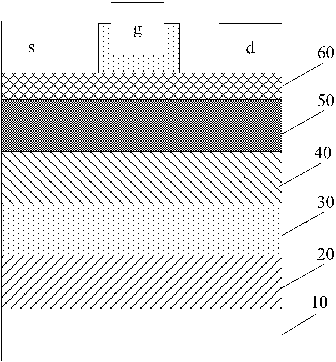
[0053] As mentioned in the background section, the breakdown voltage of existing gallium nitride semiconductor devices is relatively low.

[0054] The inventors found that this is because the existing gallium nitride semiconductor devices need to be grown using heterogeneous substrates such as sapphire or silicon, that is, gallium nitride is grown on a silicon substrate or a sapphire substrate, while a silicon substrate or a sapphire substrate and nitrogen The lattice constant of gallium nitride has a large difference. For example, the lattice constant of silicon substrate and gallium nitride has a difference of about 17%. A large number of defects are generated to form a leakage path, and gallium nitride has N-type characteristics due to its own nitrogen holes during the growth process, resulting in a low breakdown voltage of gallium nitride semiconductor devices.

[0055] In addition, since the thermal expansion coefficient of silicon substrate or sapphire substrate and gall...


PUM

PropertyMeasurementUnit
thicknessaaaaaaaaaa

Abstract

The embodiment of the invention discloses a gallium nitride semiconductor device and a manufacturing method thereof. The manufacturing method comprises the steps of growing an indium-containing bufferlayer on a first surface of a substrate, wherein the buffer layer comprises an indium-containing AlxGa<1-x>N layer, and x is greater than or equal to 0 and less than or equal to 1; forming an unintentionally doped first gallium nitride layer on the surface, which is away from the substrate, of the buffer layer; forming a second gallium nitride layer containing carbon doping on the surface, whichis away from the buffer layer, of the first gallium nitride layer; forming an unintentionally doped third gallium nitride layer on the side, which is away from the first gallium nitride layer, of thesecond gallium nitride layer; and forming an AlyGaN<1-y>N layer on the side, which is away from the second gallium nitride layer, of the third gallium nitride layer, wherein y is greater than 0 and less than or equal to 1. The gallium nitride semiconductor device manufactured by using the method can improve the breakdown voltage of the gallium nitride semiconductor device, reduce the probability of cracking of the gallium nitride semiconductor device in the manufacturing process and improve the performance of the gallium nitride semiconductor device.

Description

technical field [0001] The invention relates to the technical field of semiconductors, in particular to a method for manufacturing a gallium nitride semiconductor device, and a gallium nitride semiconductor device manufactured by the method. Background technique [0002] Compared with silicon semiconductor devices and gallium arsenide (GaAs) semiconductor devices, gallium nitride semiconductor devices have the characteristics of wide bandgap and high temperature stability. Moreover, compared with silicon semiconductor devices, gallium nitride semiconductor devices have lower temperature resistance, so that the conversion loss can be minimized during operation, and at the same time, the power consumption of the system can be minimized, making it a compact, high-voltage and high-speed The low-loss, high-efficiency new-generation power semiconductor components in the conversion field are gradually applied to industrial applications, power networks, and information and communica...

Claims


Application Information

Patent Timeline
Patent Type & Authority Applications(China)
IPC IPC(8): H01L29/772H01L29/06H01L21/30
CPCH01L29/06H01L29/772H01L21/30
Inventor 李东键金荣善金权济骆薇薇孙在亨
Owner INNOSCIENCE (ZHUHAI) TECH CO LTD
Why Eureka
Try Eureka