Fin transistor and making method thereof

A technology of a fin transistor and a manufacturing method, which is applied in the manufacturing of semiconductor/solid-state devices, semiconductor devices, electrical components, etc., can solve the problems of low thermal conductivity, high junction leakage, poor interface contact, etc., and achieve photolithography etching. The effect of simple process, improved electrical conductivity and reduced manufacturing cost

Inactive Publication Date: 2018-08-31
SHANGHAI HUALI INTEGRATED CIRCUTE MFG CO LTD
View PDF4 Cites 3 Cited by
  • Summary
  • Abstract
  • Description
  • Claims
  • Application Information

AI Technical Summary

Problems solved by technology

[0003] However, germanium (Ge) has poor thermal conductivity (thermal conductivity), that is, low thermal conductivity, poor interface contact with high dielectric constant (HK) materials (poor HK interface), and high junction leakage (junction leakage), etc. Disadvantages; In addition, it also has the disadvantage that germanium oxide (GeO, GeO2) is not a stable state (stable state)

Method used


Image

  • Fin transistor and making method thereof
  • Fin transistor and making method thereof
  • Fin transistor and making method thereof

Examples


Embodiment Construction

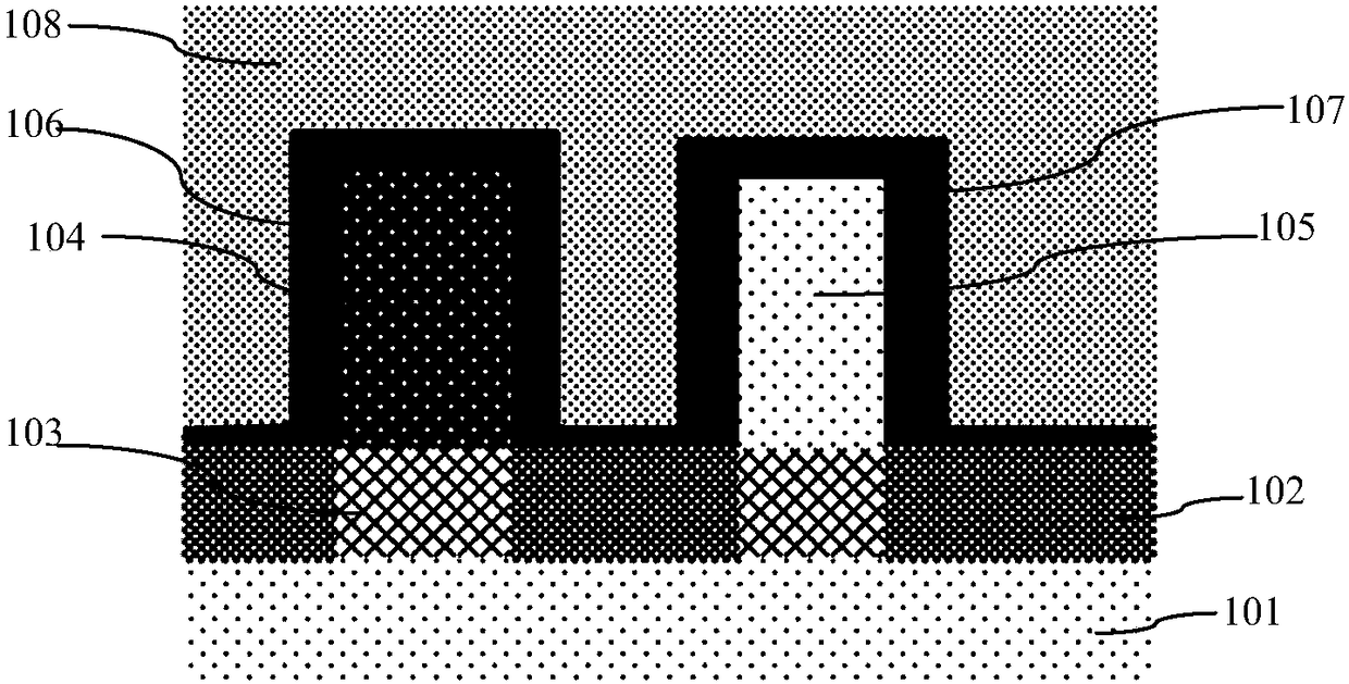
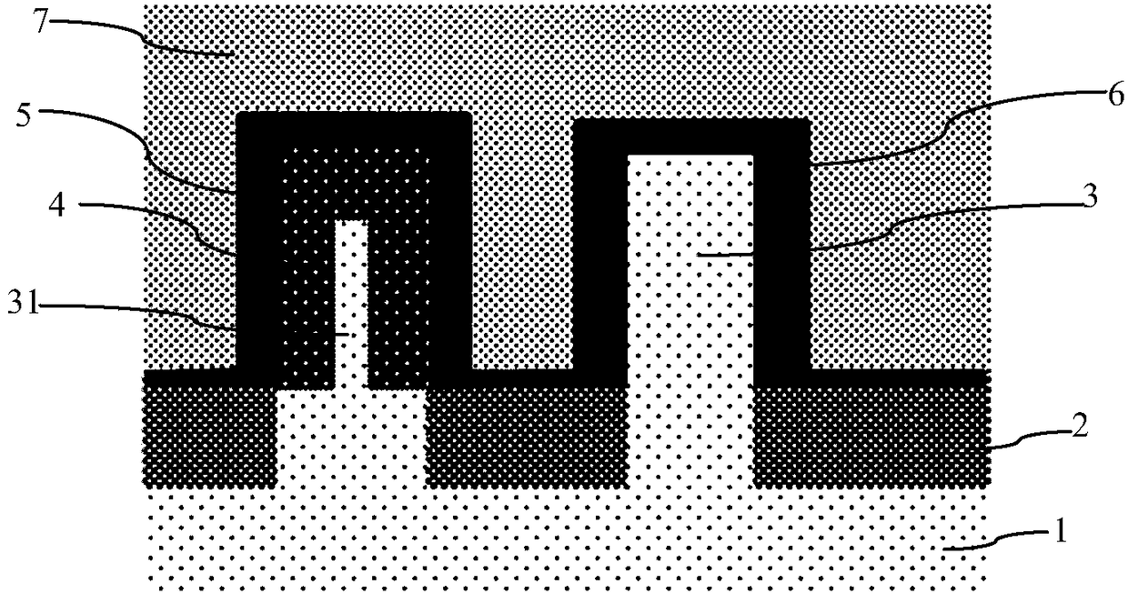
[0044] like figure 2 Shown is a cross-sectional view of the fin transistor of the embodiment of the present invention; the fin transistor of the embodiment of the present invention includes:

[0045] The silicon fin body 3 is a strip structure formed by photolithographically etching the silicon substrate 1 , and the silicon fin body 3 has an initial first width.

[0046] The bottom of the silicon fin body 3 is isolated by the first insulating layer 2 and the bottom of the silicon fin body 3 isolated by the first insulating layer 2 maintains a first width. The first insulating layer 2 is an oxide layer, for example, the first insulating layer 2 adopts shallow trench field oxygen.

[0047] A source region and a drain region are formed in the silicon fin body 3, and the formation regions of the source region and the drain region are automatically formed by dummy gates covering the top surface and side surfaces of the silicon fin body 3 having a first width. Alignment definitio...


PUM


Abstract

The invention discloses a fin transistor comprising a silicon fin body with an initial first width. The bottom of the silicon fin body is isolated by a first insulation layer. A source region and a drain region are formed in the silicon fin body. After pseudo grid removing and before metal gate structure forming, isotropic etching type thinning is carried out on the silicon fin body exposed by anarea with the pseudo grid removed; and a germanium-silicon epitaxial layer coats the lateral surface and the top surface of the thinned silicon fin body by epitaxial growth, wherein the germanium concentration of the germanium-silicon epitaxial layer is in gradient distribution. The metal gate structure covers the top surface and the lateral surface of the germanium-silicon epitaxial layer and thegermanium-silicon epitaxial layer forms a channel region. In addition, the invention also discloses a making method of a fine transistor. Therefore, the channel region is formed by using a germaniumsilicon material without the need to use the silicon germanium fin body separately, so that the conductive performance of the device is improved; and no SRB layer is need, so that the cost is loweredand the process is simplified.

Description

technical field [0001] The invention relates to the field of semiconductor integrated circuit manufacturing, in particular to a fin transistor (FinFET transistor). The invention also relates to a method for manufacturing a fin transistor. Background technique [0002] With the continuous development of semiconductor technology, the process flow after the process node reaches 10nm may introduce silicon germanium (SiGe) x Ge 1-x ) or pure germanium (pure Ge) as the channel region (channel) material. The main reason is that the electron mobility and hole mobility of germanium are 2.5 times and 4 times that of silicon (Si), respectively, which can greatly increase the driving current under the condition of reducing the operating voltage. [0003] However, germanium (Ge) has poor thermal conductivity (thermal conductivity), that is, low thermal conductivity, poor interface contact with high dielectric constant (HK) materials (poor HK interface), and high junction leakage (junc...

Claims


Application Information

Patent Timeline
IPC IPC(8): H01L29/78H01L21/8234H01L21/336
CPCH01L29/785H01L21/823431H01L29/66795
Inventor 许佑铨
Owner SHANGHAI HUALI INTEGRATED CIRCUTE MFG CO LTD
Why Eureka
Try Eureka