

A chip bonding device and method
A chip bonding and bonding device technology, applied in semiconductor devices, electrical components, circuits, etc., can solve problems such as low accuracy and yield, and achieve the effects of improving yield, saving operating time, and saving plant area.
- Summary
- Abstract
- Description
- Claims
- Application Information
AI Technical Summary
Problems solved by technology
Method used
Image

Examples
Embodiment 1
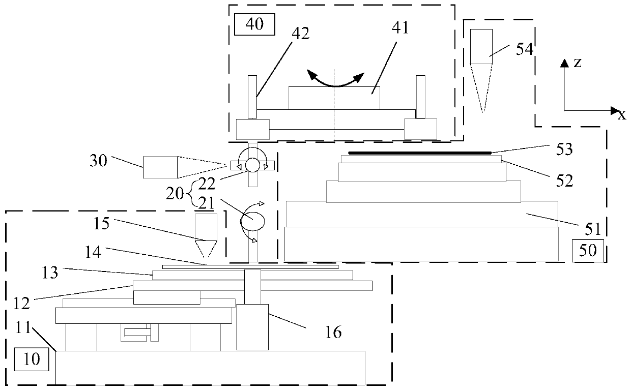
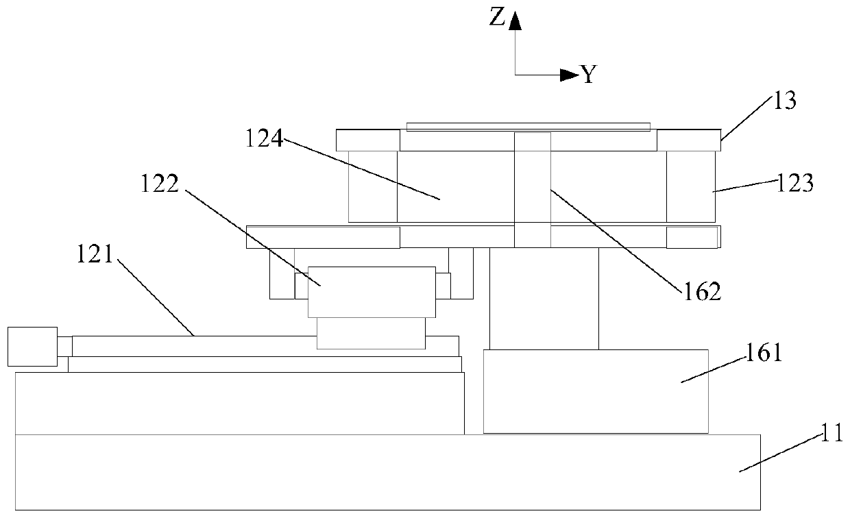
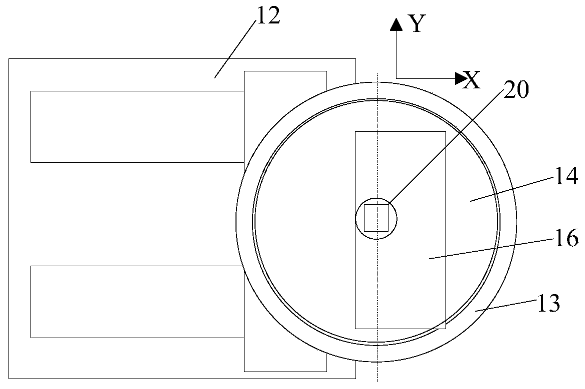
[0047] like figure 1 As shown, a chip bonding device includes a chip supply unit 10, a chip pick-up unit 20, a chip measurement unit 30, a chip temporary carrying unit 40 and a chip bonding unit 50 corresponding in sequence, and the chip temporary carrying unit 40 includes a carrying Turntable 41, bonding hands 42 distributed on the carrying turntable 41 along the circumferential direction, the chip pick-up unit 20 picks up the chip on the chip supply unit 10, and after alignment by the chip measurement unit 30, handover to the The bonding hand 42 receives the chip and transfers it to the chip bonding unit 50 for bonding with the substrate carried on the chip bonding unit 50 . Specifically, the chip supply unit 10, the chip pick-up unit 20, the chip measurement unit 30, the chip temporary carrying unit 40 and the chip bonding unit 50 adopt a three-dimensional layout. In this embodiment, the chip supply unit 10 is located at the bottom, and the chip temporary carrying unit 40 ...
Embodiment 2
[0063] like Figure 4 As shown, the difference from Embodiment 1 is that when the chip mark is in a die-down bonding mode, the chip pick-up unit 20 includes a pick-up hand 21, and the pick-up hand 21 picks up the chip from the chip supply unit 10, The rotation reaches the measuring station and the handover station of the temporary chip carrying unit in sequence, and is transmitted to the bonding hand 42 , and the measuring station corresponds to the chip measuring unit 30 . Specifically, the pick-up hand 21 picks up the chip from the chip supply unit 10, and first rotates to the measurement station, and the chip measurement unit 30 aligns the chip, that is, measures and aligns the alignment marks on the chip. After quasi-finishing, the picking hand 21 carries the chip and continues to rotate to the handover station of the chip temporary carrying unit, and handover the chip to the bonding hand 42 .
[0064] The pick-up hand 21 can move vertically between the chip supply unit 1...
Embodiment 3
[0066] like Figure 5As shown, the difference from Embodiment 1 is that when the chip mark is in a die-down bonding mode, the chip pick-up unit 20 includes a pick-up hand 21, a turning hand 22 and a delivery hand 23 arranged in sequence from bottom to top. , the pick-up hand 21 picks up the chip from the chip supply unit 20, rotates and transfers it to the flipping hand 23, and the flipping hand 23 rotates in turn to reach the measurement station and transfer hand transfer station, and the transfer hand 23 absorbs the The chip is handed over to the bonding hand 42 , and the measuring station corresponds to the chip measuring unit 30 . Specifically, the pick-up hand 21 picks up the chip from the chip supply unit 10, and rotates to the turning hand handover station. The turning hand 22 receives the chip and first rotates to the measuring station, and the chip measuring unit 30 checks the chip. Alignment, after the alignment is completed, the turning hand 22 continues to rotate ...
PUM
 Abstract
Description
Claims
Application Information