Grid manufacturing method

A manufacturing method and gate technology, applied in the field of gate manufacturing, can solve the problems of photoresist 206 loss, active region damage, polysilicon gate damage, etc., and achieve the effect of planarization

Active Publication Date: 2018-09-11
SHANGHAI HUALI INTEGRATED CIRCUTE MFG CO LTD
View PDF8 Cites 11 Cited by
  • Summary
  • Abstract
  • Description
  • Claims
  • Application Information

AI Technical Summary

Problems solved by technology

In the process of etching back the oxide layer 105, the photoresist 206 has a certain loss. When the oxide layer 105 on the top of some gates has not been removed, the height of part of the photoresist 206 is already lower than the height of the polysilicon gate 103. , thus exposing the sides of the polysilicon gate 103
The transition loss of the photoresist 206 caused by the excessive height difference of the gate is likely to cause damage to the active region and the polysilicon gate, which will affect the electrical properties of the original.

Method used


Image

  • Grid manufacturing method
  • Grid manufacturing method
  • Grid manufacturing method

Examples


Embodiment Construction

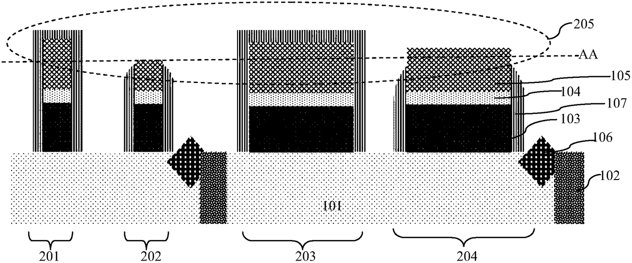
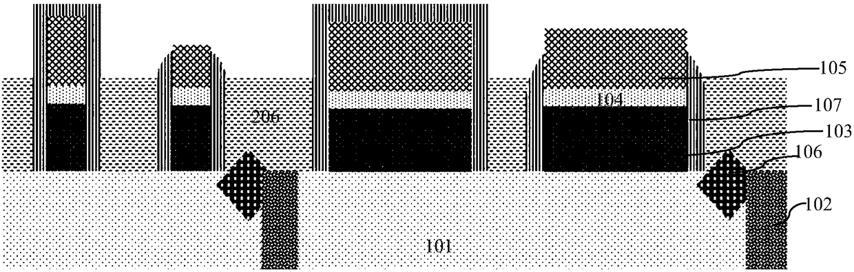
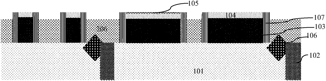
[0041] like image 3 Shown is the flow chart of the method of the embodiment of the present invention; Figure 4A to Figure 4GAs shown, it is a device structure diagram in each step of the method of the embodiment of the present invention. The manufacturing method of the gate of the embodiment of the present invention includes the following steps:

[0042] Step 1, such as Figure 4A As shown, a semiconductor substrate 1 is provided, and a gate dielectric layer and a polysilicon gate 3 are sequentially formed on the surface of the semiconductor substrate 1 .

[0043] The semiconductor substrate 1 is a silicon substrate.

[0044] The gate dielectric layer is a gate oxide layer.

[0045] A field oxide layer 2 is formed in the semiconductor substrate 1 , and an active region is isolated by the field oxide layer 2 . The field oxide layer 2 is shallow trench field oxide, which is formed by a shallow trench isolation process.

[0046] The active area includes an active area corr...


PUM


Abstract

The invention discloses a grid manufacturing method. The grid manufacturing method comprises the steps of: forming a grid dielectric layer and a polysilicon grid; forming a hard mask layer superposedby a first nitride layer and a second oxide layer; forming a grid through photolithography etching; forming a nitride layer sidewall on a side surface of the grid; forming a nitride layer contact holeetching stop layer; forming an oxide layer interlayer film; performing a first chemical mechanical polishing of the oxide layer by using the contact hole etching stop layer as a stop layer; performing nitride layer etching to remove the nitride layer on the top of the second oxide layer of each grid; etching the oxide layer to remove the second oxide layer on the top of the grid, wherein the thickness of the interlayer film is synchronously reduced; using the polysilicon grid as a stop layer to perform a second chemical mechanical polishing on the remaining nitride and oxide layers above thetop surface of the polysilicon grid. The invention can realize stable control of the height of the grid, can improve the consistency of the grid height, does not require a photomask, and is low in cost.

Description

technical field [0001] The invention relates to a method for manufacturing a semiconductor integrated circuit, in particular to a method for manufacturing a grid. Background technique [0002] In the existing advanced logic chip technology, components usually include n-type field effect transistors (FETs) or nFETs and p-type field effect transistors or pFETs. In order to increase the electrical performance of components, an additional component enhancement process is performed in addition to the pFET or nFET process. These component enhancement processes will directly affect the gate heights of various subsequent components, resulting in differences in the gate heights between different subsequent components and affecting the electrical properties of the components. like figure 1 As shown, it is a structural diagram of a gate formed by a conventional gate manufacturing method; a field oxide layer 102 is formed on a semiconductor substrate such as a silicon substrate 101, an...

Claims


Application Information

Patent Timeline
Patent Type & Authority Applications(China)
IPC IPC(8): H01L21/8238
CPCH01L21/823828
Inventor 李镇全
Owner SHANGHAI HUALI INTEGRATED CIRCUTE MFG CO LTD
Why Eureka
Try Eureka