

A kind of high-quality gan thin film and preparation method thereof
A high-quality, thin-film technology, applied in the direction of semiconductor devices, semiconductor lasers, electrical components, etc., can solve problems such as unstable structures, high pressure, and complex processes, and achieve the effects of stress reduction, performance improvement, and crystal quality improvement
- Summary
- Abstract
- Description
- Claims
- Application Information
AI Technical Summary
Problems solved by technology
Method used
Image


Examples
Embodiment 1
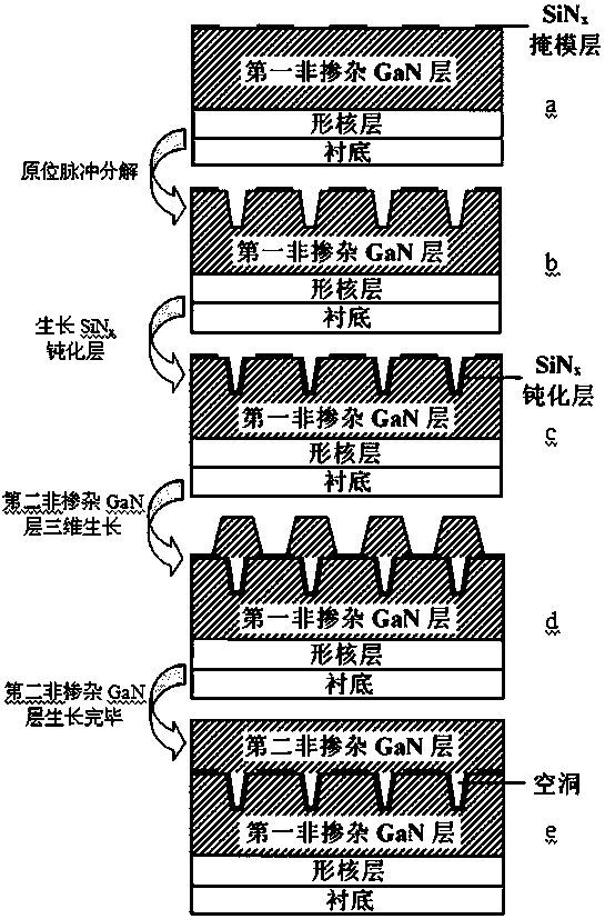
[0030] High-quality GaN thin film preparation methods, such as figure 1 shown, including the following steps:
[0031] first step, such as figure 1 As shown in a, by the in-situ growth method, the nucleation layer, the first non-doped GaN layer, the SiN x mask layer, wherein the growth temperature of the nucleation layer is 500°C; the growth temperature of the first non-doped GaN layer is 1000°C, and the thickness is 100nm; the SiN x The growth temperature of the mask layer is 1050°C, and the thickness is 10nm;
[0032] In the second step, the sample obtained in the first step was placed in NH at 900°C 3 and H 2 In situ pulse decomposition in a mixed atmosphere, NH 3 Turn on for 20s, pause for 20s, cycle 15 times, H 2 Continuous access, after 10min, will get image 3 As shown in the morphology, the first non-doped GaN layer has a porous structure;
[0033] The third step is to grow SiN on the epitaxial structure obtained in the second step x Passivation layer, the gro...
Embodiment 2
[0037] High-quality GaN thin film preparation methods, such as figure 1 shown, including the following steps:
[0038] first step, such as figure 1 As shown in a, by the in-situ growth method, the nucleation layer, the first non-doped GaN layer, the SiN x mask layer, wherein the growth temperature of the nucleation layer is 530°C; the growth temperature of the first non-doped GaN layer is 1050°C, and the thickness is 3μm; the SiN x The growth temperature of the mask layer is 1050°C, and the thickness is 50nm;
[0039] In the second step, the sample obtained in the first step is placed in NH at 1000°C 3 and H 2 In situ pulse decomposition in a mixed atmosphere, NH 3 Turn on for 60s, pause for 60s, cycle 10 times, H 2 Continuous access, after 20min, will get Figure 4 As shown in the morphology, the first non-doped GaN layer has a porous structure;
[0040]The third step is to grow SiN on the epitaxial structure obtained in the second step x Passivation layer, the growt...
Embodiment 3
[0044] High-quality GaN thin film preparation methods, such as figure 1 shown, including the following steps:
[0045] first step, such as figure 1 As shown in a, by the in-situ growth method, the nucleation layer, the first non-doped GaN layer, the SiN x mask layer, wherein the growth temperature of the nucleation layer is 570°C; the growth temperature of the first non-doped GaN layer is 1100°C, and the thickness is 5 μm; the SiN x The growth temperature of the mask layer is 1050°C, and the thickness is 100nm;
[0046] In the second step, the sample obtained in the first step is placed in NH at 1100°C 3 and H 2 In situ pulse decomposition in a mixed atmosphere, NH 3 Enter 45s, pause 45s, cycle 20 times, H 2 Continuous access, after 30min, will get Figure 5 As shown in the morphology, the first non-doped GaN layer has a porous structure;
[0047] The third step is to grow SiN on the epitaxial structure obtained in the second step x Passivation layer, the growth tempe...
PUM
 Abstract
Description
Claims
Application Information