Electrode structure capable of enhancing luminous efficiency, QLED and preparation method of electrode structure capable of enhancing luminous efficiency

A technology of electrode structure and light extraction efficiency, applied in circuits, electrical components, electric solid devices, etc., can solve the problem of inability to improve the light extraction efficiency of QLED devices, and achieve the goal of reducing the probability of total reflection, improving hole injection efficiency, and improving light extraction efficiency. Effect

Active Publication Date: 2018-09-14
TCL CORPORATION
View PDF9 Cites 2 Cited by
  • Summary
  • Abstract
  • Description
  • Claims
  • Application Information

AI Technical Summary

Problems solved by technology

[0005] In view of the above-mentioned deficiencies in the prior art, the purpose of the present invention is to provide an electrode structure, QLED and preparation method that can improve the light extraction efficiency, aiming at solving the problem that the existing electrode structure cannot improve the light extraction efficiency of the QLED device

Method used


Image

  • Electrode structure capable of enhancing luminous efficiency, QLED and preparation method of electrode structure capable of enhancing luminous efficiency
  • Electrode structure capable of enhancing luminous efficiency, QLED and preparation method of electrode structure capable of enhancing luminous efficiency
  • Electrode structure capable of enhancing luminous efficiency, QLED and preparation method of electrode structure capable of enhancing luminous efficiency

Examples


Embodiment 1

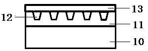
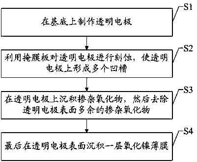
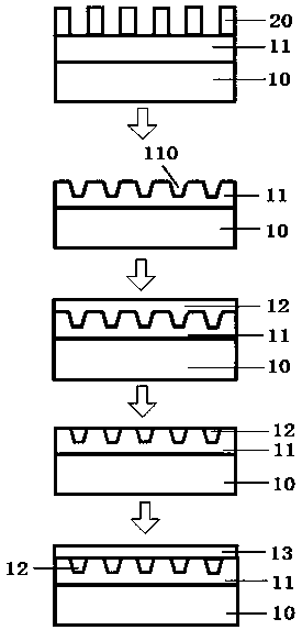
[0048] Clean the substrate, deposit a 250nm ITO film on the substrate by magnetron sputtering, deposit a layer of positive photoresist on the ITO film, and use it as a mask after exposure and development to control the aperture of the circular hole on the mask The total area of ​​the circular holes accounts for 15% of the total surface area of ​​the mask. The ITO thin film was etched by wet method, and the etching depth was controlled to be 100nm. Expose to remove the mask, and then use the magnetron sputtering method to deposit a 200nm AZO film on the ITO film, and then use chemical mechanical polishing to remove the AZO film on the surface of the ITO film, leaving only a 200nm ITO film on the substrate. At this time, about 50 nm of AZO was filled into the grooves of the ITO film. Finally, a 7.5nm NiO film was deposited on the surface of the ITO film by magnetron sputtering. A hole injection layer, a hole transport layer, a quantum dot light-emitting layer, an electron tran...

Embodiment 2

[0050] The substrate was cleaned, and a 300nm ITO film was deposited on the substrate by magnetron sputtering, and a plurality of circular grooves were etched by laser (the groove diameter was 5 μm, and the total area of ​​the grooves accounted for 20% of the total surface area of ​​the mask. %), control the etching depth to 50nm. A 200nm FTO film was deposited on the ITO film by magnetron sputtering, and then chemical mechanical polishing was used to remove the FTO film on the surface of the ITO film, leaving only a 200nm ITO film on the substrate. At this time, about 50 nm of FTO was filled in the grooves of the ITO film. Finally, a 10nm MnO film was deposited on the surface by magnetron sputtering. A hole injection layer, a hole transport layer, a quantum dot light-emitting layer, an electron transport layer, an electron injection layer, and a cathode are sequentially deposited on the MnO thin film to obtain a QLED device.

Embodiment 3

[0052] Clean the substrate, deposit a 275nm ITO film on the substrate by magnetron sputtering, deposit a layer of positive photoresist on the ITO film, and use it as a mask after exposure and development to control the aperture of the circular hole on the mask The total area of ​​the circular holes accounts for 30% of the total surface area of ​​the mask. The ITO thin film was etched by wet method, and the etching depth was controlled to be 75nm. The mask was removed by exposure, and a 200nm ATO film was deposited on the ITO film by magnetron sputtering, and then chemical mechanical polishing was used to remove the ATO on the surface of the ITO film, leaving only a 200nm ITO film on the substrate. At this time, about 50 nm of ATO was filled in the grooves of the ITO thin film. Finally, a 5nm NiO film was deposited on the surface by magnetron sputtering. A hole injection layer, a hole transport layer, a quantum dot light-emitting layer, an electron transport layer, an electro...


PUM

PropertyMeasurementUnit
depthaaaaaaaaaa
thicknessaaaaaaaaaa
thicknessaaaaaaaaaa

Abstract

The invention discloses an electrode structure capable of enhancing luminous efficiency, a QLED and a preparation method of the electrode structure capable of enhancing the luminous efficiency. The electrode structure comprises a substrate, a transparent electrode which is arranged on the surface of the substrate and has multiple slots, a doped oxide filling in the slots and a nickel oxide film ora manganese oxide film which is deposited on the surface of the transparent electrode. According to the electrode structure, the doped oxide is introduced to the transparent electrode having the slots to fill in the slots and then a layer of nickel oxide film or manganese oxide film is deposited on the transparent electrode, the light emitted out of the luminous layer can be effectively constrained by introducing of the nickel oxide film or the manganese oxide film, the light can be guided into the slots of the transparent electrode to a greater extent, and the light emergent angle of the light from the transparent electrode to the glass interface can be changed by using the slots and the probability of total reflection can be reduced so that the luminous efficiency of the device can be enhanced. The barrier of the transparent electrode and the luminous functional layer can be reduced and the hole injection efficiency of the device can be enhanced.

Description

technical field [0001] The invention relates to the field of light emitting displays, in particular to an electrode structure capable of improving light extraction efficiency, a QLED and a preparation method. Background technique [0002] Quantum dot light-emitting diodes (QLEDs) are considered to be an advantageous technology for next-generation light-emitting devices due to their advantages of saturated color, high purity, good monochromaticity, adjustable color, and preparation by solution method. At present, the external quantum efficiency of QLED can only reach 20% or even lower, and most of the light is confined in the device structure, which is mainly due to the adaptation of the refractive index of the QLED device structure. When propagating through high-rate materials (such as ITO / glass interface, glass / air interface), a large part of the light is captured, the ITO / glass interface is called waveguide mode total reflection, and the glass / air interface is called glass...

Claims


Application Information

Patent Timeline
Patent Type & Authority Applications(China)
IPC IPC(8): H01L51/52
CPCH10K50/805H10K50/813H10K50/816H10K50/85H10K50/858
Inventor 张滔向超宇李乐辛征航张东华
Owner TCL CORPORATION
Why Eureka
Try Eureka