Circuit board partition block seamless laser processing method for thick gas electron multiplier

A technology of gas electron multiplication and laser processing method, which is applied in the direction of printed circuit, printed circuit manufacturing, electrical components, etc., can solve the problems such as the decrease of the concentricity between the insulating ring and the through hole, the etching of the insulating ring is not clean, and the impact on the product yield. Achieve the effects of reducing processing complexity and material consumption, avoiding insulation etching failure, and avoiding quality hazards

Active Publication Date: 2018-09-18
HUIZHOU KING BROTHER CIRCUIT TECH +1
View PDF3 Cites 0 Cited by
  • Summary
  • Abstract
  • Description
  • Claims
  • Application Information

AI Technical Summary

Problems solved by technology

This process needs to be combined with a laser lithography system with high positioning accuracy, the cost is high, and its rim can also reach 100μm
The fourth such as figure 1 As shown in middle d, no protective film is covered, and the entire plate is directly etched after mechanical drilling, so that the thickness of the copper layer will decrease with the increase of the rim size, and the control is relatively difficult
Too thin board or too soft board will have large board size expansion and contraction, and the precision is difficult to control, especially after multiple processes, the concentricity of the insulating ring and the through hole will drop significantly
However, if the plate is too thick, the laser processing energy needs to be increased. For the double positioning processing mode, if the laser energy is too large, the insulating ring will not be etched clean, and even the hole wall will be severely carbonized, which will affect the yield of the product.

Method used


Image

  • Circuit board partition block seamless laser processing method for thick gas electron multiplier
  • Circuit board partition block seamless laser processing method for thick gas electron multiplier
  • Circuit board partition block seamless laser processing method for thick gas electron multiplier

Examples


Embodiment 1

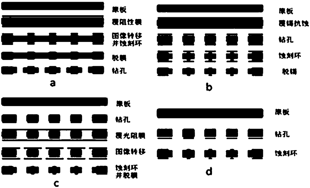
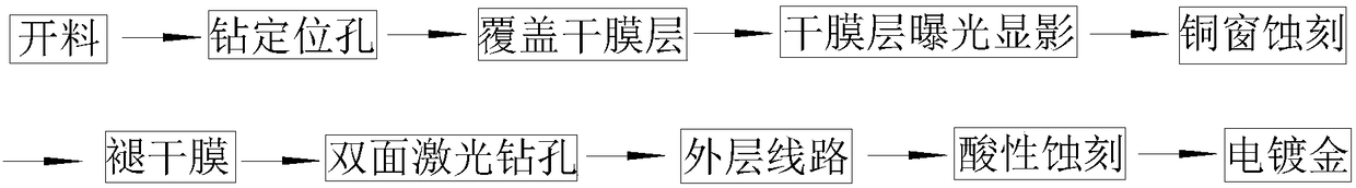
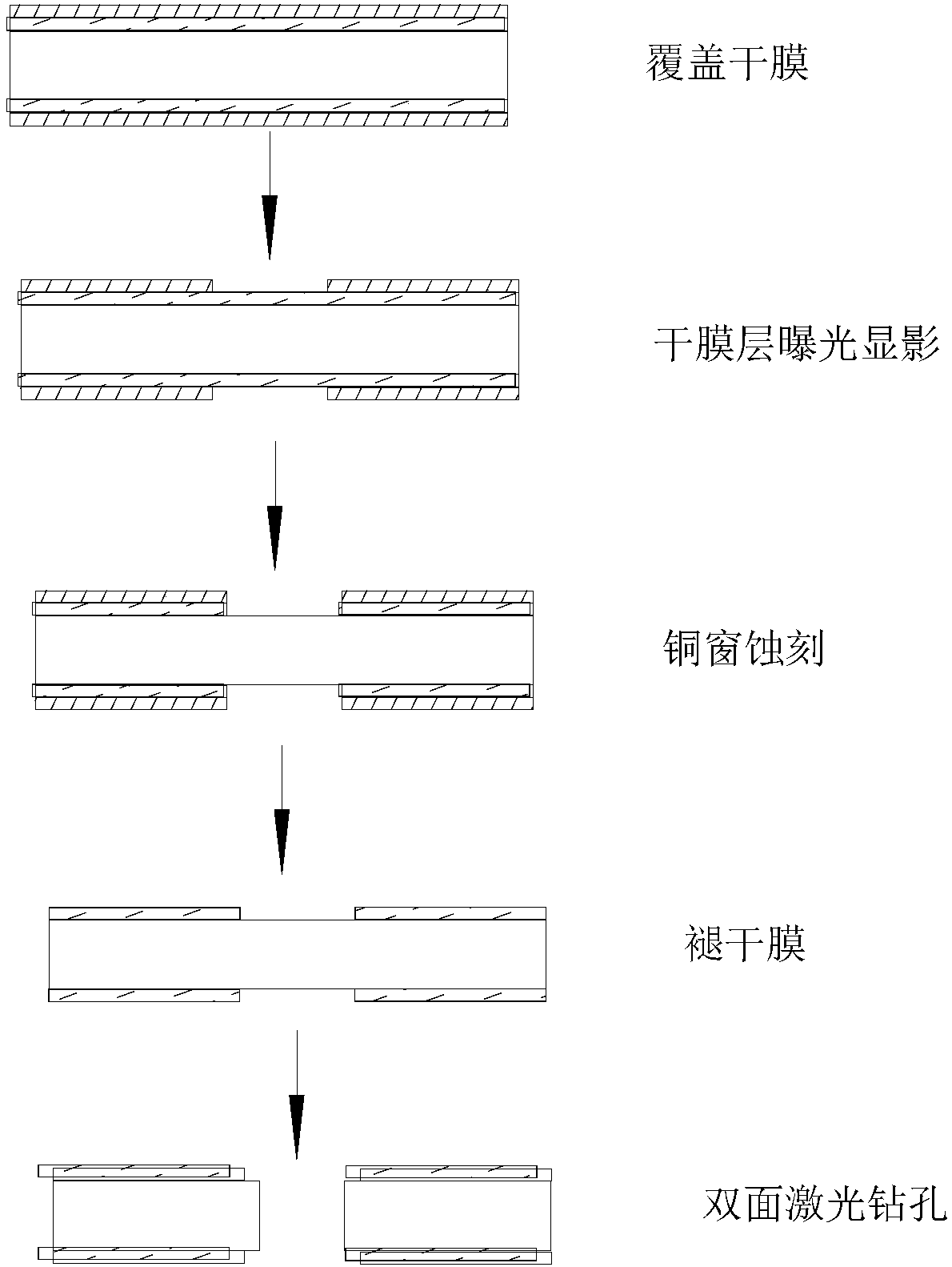
[0036] like figure 2 , image 3 and Figure 4 As shown, the block-by-block seamless laser processing method for a thick gas electron multiplier circuit board includes the following steps:

[0037] 1) According to the design requirements, the original plate is obtained, and the laser drilling area 2 is designed on the upper surface of the original plate, and the laser drilling area 2 is divided into four blocks 3; the block 3 and the adjacent block 3 For seamless splicing and connection, the side legs of block 3 are provided with alignment points 4;

[0038] 2) Drill positioning holes on the original plate obtained in step 1) cutting;

[0039] 3) Cover the dry film layer with the original plate treated in step 1), and expose and develop the dry film layer;

[0040] 4) Carry out the copper window etching of the original plate after step 3) and take off the dry film;

[0041] 5) Perform double-sided laser drilling on block 3 on the original plate after step 4) regardless of...


PUM


Abstract

The invention discloses a circuit board partition block seamless laser processing method for a thick gas electron multiplier. The method comprises steps that 1), rough shape cutting is carried out according to design requirements to acquire an original plate; 2) a positioning hole is drilled in the original plate acquired through rough shape cutting in the step 1); 3) the original plate after treatment in the step 1) is covered with a dry film layer, and the dry film layer is exposed and developed; 4) the original plate after treatment in step 3) is subjected to copper window etching, and a dry film is removed; 5) laser drilling on the original plate after treatment in the step 4) is carried out; 6), an outer layer line is prepared on the original plate after treatment in the step 5), andacid etching is carried out; and 7), gold plating on the surface of the original plate after treatment in the step 6) is carried out. The method is advantaged in that product quality is improved, compatibility is improved, and production difficulty is reduced.

Description

technical field [0001] The invention relates to a method for manufacturing a circuit board for a thick gas electron multiplier, in particular to a segmented block seamless laser processing method for a circuit board for a thick gas electron multiplier. Background technique [0002] Thick GEM, Thick gaseous electron multiplier (Thick gaseous electron multiplier, THGEM) is a new structure gas detector developed on the basis of traditional GEM. The basic structure of the GEM detector is: an array of tiny holes is made on an insulating plate covered with a thin conductive metal layer on the upper and lower surfaces. Due to the existence of the microporous structure, when a certain voltage difference is applied to the electrodes on the upper and lower planes, a strong electric field can be formed in the hole. When the microporous structure is in a specific working gas, if ionized electrons appear around the pores, the electron avalanche multiplication process can occur in the wo...

Claims


Application Information

Patent Timeline
Patent Type & Authority Applications(China)
IPC IPC(8): H05K3/00
CPCH05K3/00
Inventor 武守坤谢宇广吴军权陈春林映生林鹭华唐宏华乔元闫文奇孙丽君
Owner HUIZHOU KING BROTHER CIRCUIT TECH
Why Eureka
Try Eureka