GaN-based LED structure and preparation method thereof

An LED structure, N-type technology, used in electrical components, circuits, semiconductor devices, etc., can solve problems such as restricting development, LED luminous efficiency attenuation, and restricting the development of high-power LEDs.

Active Publication Date: 2018-09-28
ELEC TECH OPTOELECTRONICS TECHWUHUCO
View PDF6 Cites 2 Cited by
  • Summary
  • Abstract
  • Description
  • Claims
  • Application Information

AI Technical Summary

Problems solved by technology

[0003] With the increasing application range of LEDs in the lighting and backlighting markets year by year, the application demand for medium and high power devices has increased significantly. However, LEDs have the problem of attenuation of luminous efficiency under high current injection, which limits the development of high-power LEDs to a certain extent. Restricted the development of LED in the field of general lighting

Method used


Image

  • GaN-based LED structure and preparation method thereof
  • GaN-based LED structure and preparation method thereof

Examples


preparation example Construction

[0041] The embodiment of the present invention also provides a method for preparing the GaN-based LED structure, comprising the following steps:

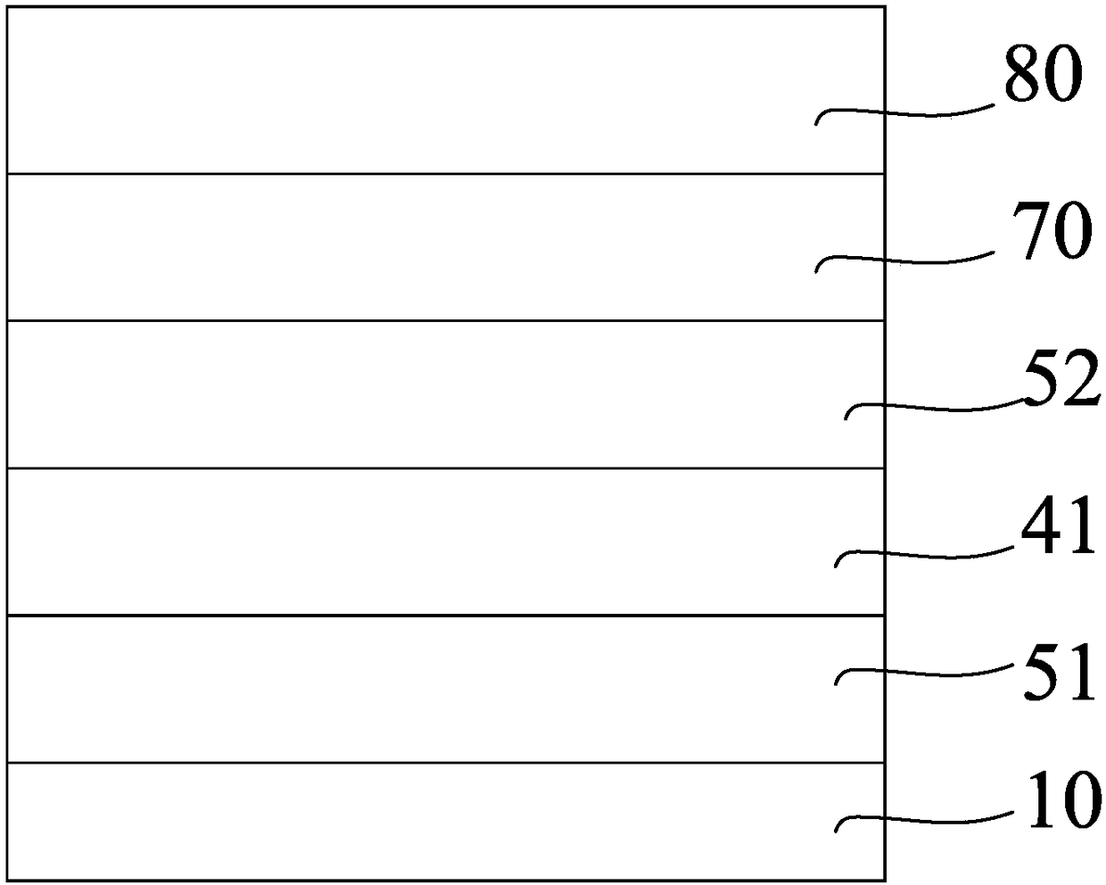
[0042] providing a substrate 10; and

[0043] On the substrate 10, the first N-type doped GaN layer 51, the first ZnGeN 2 The barrier layer 41 , the second N-type doped GaN layer 52 , the multi-quantum well layer 70 and the P-type doped GaN layer 80 .

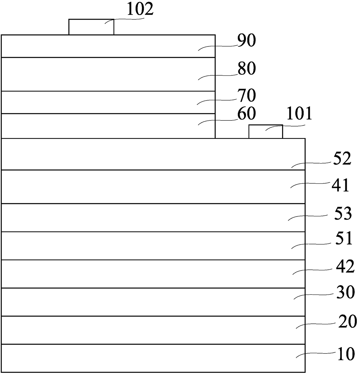
[0044] In one embodiment, before growing the first N-type doped GaN layer 51, the following steps are further included:

[0045] epitaxially growing a buffer layer 20 on said substrate 10; and

[0046] epitaxially grow a second ZnGeN on the buffer layer 20 2 barrier layer 42 .

[0047] The growth temperature of the buffer layer may range from 950°C to 1050°C. In one embodiment, after the buffer layer 30 and before growing the first N-type doped GaN layer 51 , a step of growing a leveling layer is further included. The growth temperature of the leveling layer 30 may be 1050°C-11...

Embodiment

[0057] (1) providing a sapphire substrate 10;

[0058] (2) Cu is evaporated onto the sapphire substrate 10 by electron beam deposition (PVD);

[0059] (3) grow a layer of 20nm graphene layer under the condition of 540 DEG C by chemical vapor deposition (CVD);

[0060] (4) feed ammonia gas, hydrogen gas and trimethylgallium, and grow a 20nm buffer layer 20 on the graphene layer at 1000°C;

[0061] (5) inject ammonia gas, hydrogen gas and trimethylgallium, and grow a 1.5 μm leveling layer 30 on the buffer layer 20 at 1080° C.;

[0062] (6) Feed ammonia gas, hydrogen gas, Zn metal vapor and Ge metal vapor, grow the second ZnGeN of 5.5nm on the buffer layer 30 at 900°C 2 barrier layer 42;

[0063] (7) into silane (SiH 4 ), ammonia gas, hydrogen gas and trimethylgallium, growing a 0.8um first doped N-type doped GaN layer 51 on the buffer layer 20 at 1080°C;

[0064] (8) into silane (SiH 4 ), ammonia gas, hydrogen gas and trimethylgallium, and grow the third doped N-type doped...


PUM

PropertyMeasurementUnit
thicknessaaaaaaaaaa
thicknessaaaaaaaaaa
thicknessaaaaaaaaaa

Abstract

The invention discloses a GaN-based LED structure, which sequentially comprises a substrate, a first N-type doped GaN layer, a first ZnGeN2 barrier layer, a second N-type doped GaN layer, a multi-quantum well layer and a P-type doped GaN layer from bottom to top. The invention also discloses a preparation method of the GaN-based LED structure.

Description

technical field [0001] The invention relates to the field of light-emitting diodes, in particular to a GaN-based LED structure and a preparation method thereof. Background technique [0002] A light-emitting diode (Light-Emitting Diode, LED) is a semiconductor electronic component capable of emitting light. It is very popular because of its small size, low energy consumption, long life, and low driving voltage, and is widely used in indicator lights, display screens, etc. The pursuit of high brightness and high performance has become a trend. In order to meet the growing demand, it is imminent to improve the luminous efficiency of LED chips. LED lighting has become an obvious trend to replace traditional lighting, and LED lighting will enter a period of rapid growth. The key to the popularization of LED lighting lies in the improvement of blue-ray LED epitaxial chip technology. The breakthrough and development of technology will drive the improvement of lighting brightness...

Claims


Application Information

Patent Timeline
Patent Type & Authority Applications(China)
IPC IPC(8): H01L33/14H01L33/16H01L33/00
CPCH01L33/0066H01L33/0075H01L33/145H01L33/16
Inventor 李若雅汪琼祝庆陈柏君陈柏松
Owner ELEC TECH OPTOELECTRONICS TECHWUHUCO
Why Eureka
Try Eureka