
AlGaN-based deep ultraviolet light emitting diode device structure and preparation method thereof

A technology for light-emitting diodes and device structures, applied in semiconductor devices, electrical components, circuits, etc., can solve the problems of uneven injection and low carrier injection efficiency, reduce the polarization charge density, solve the Droop effect, and reduce the potential The effect of base height

Pending Publication Date: 2022-04-19
PEKING UNIV
View PDF3 Cites 0 Cited by
  • Summary
  • Abstract
  • Description
  • Claims
  • Application Information

AI Technical Summary

Problems solved by technology

[0007] The present invention proposes a new AlGaN-based deep ultraviolet (DUV) light-emitting device structure, which can effectively solve the problems of low carrier injection efficiency, uneven injection and Droop effect under high current in the deep ultraviolet LED structure

Method used


Image

  • AlGaN-based deep ultraviolet light emitting diode device structure and preparation method thereof
  • AlGaN-based deep ultraviolet light emitting diode device structure and preparation method thereof

Examples


Embodiment 1

[0054] Example 1 Preparation of High Injection Efficiency Deep Ultraviolet LED Structure Using Sidewalls

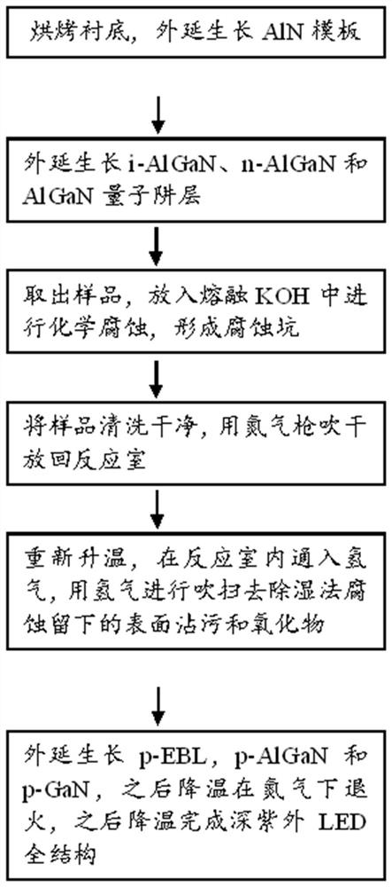
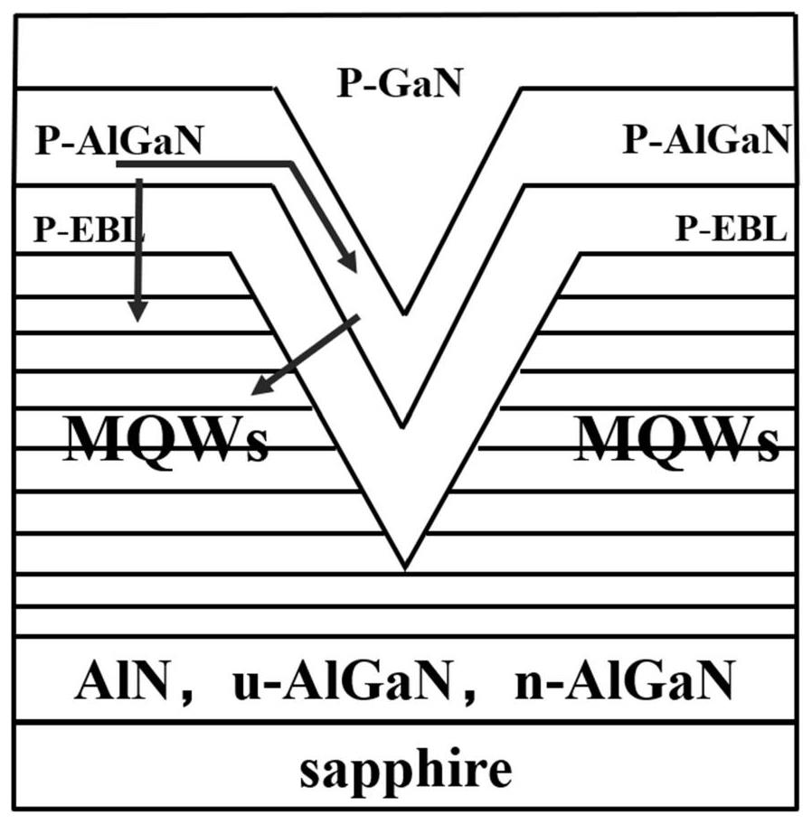
[0055] This embodiment provides a method for preparing a high-injection-efficiency deep-ultraviolet LED structure utilizing the sidewall of a V-shaped etching pit, such as figure 1 shown, including:

[0056] S1: Put the (0001) plane sapphire substrate in the reaction chamber of MOCVD equipment (3×2”Aixtron CCS FP-MOCVD), and pass H 2 , the reaction chamber pressure was 40mbar, baked at 1100°C for 300s, cleaned the substrate and lowered the temperature to 930°C, fed ammonia gas and TMAl to grow the AlN nucleation layer of 10nm, then raised the temperature to 1250°C, and epitaxially grown AlN with a thickness of 1 micron ;

[0057] Then the temperature was lowered to 1160°C, and ammonia gas, TMAl and TMGa were introduced to grow 20 cycles of Al 0.6 Ga 0.4 AlGaN with an Al composition of 0.6 and a thickness of 300 nanometers (ie i-AlGaN) is grown after the N / AlN stress a...


PUM

PropertyMeasurementUnit
thicknessaaaaaaaaaa
depthaaaaaaaaaa

Abstract

The invention relates to the field of compound semiconductor optoelectronic devices, in particular to a device structure of a high-performance AlGaN-based deep ultraviolet light-emitting diode (LED) device and a preparation method of the device structure. The AlGaN-based deep ultraviolet light emitting diode device structure provided by the invention is provided with a V-shaped three-dimensional p-n junction injection structure. And the V-shaped three-dimensional p-n junction injection structure is formed by further forming an AlGaN electron barrier layer (EBL), a p-AlGaN and a p-GaN contact layer on the semi-polar surface of the side wall of the V-shaped corrosion pit of the AlGaN-based quantum well part. According to the V-shaped three-dimensional p-n junction injection structure, the inherent limitation that holes in an AlGaN-based deep ultraviolet LED which is widely used at present and grows on a (0001) plane sapphire substrate can only be injected in the [000-1] direction is changed, so that the problem of low injection efficiency caused by insufficient hole migration capability is effectively solved, and the hole concentration and uniform distribution in an LED device quantum well are remarkably improved; therefore, the light output power of the device is improved, and meanwhile, the Droop effect problem under large current injection is effectively solved.

Description

technical field [0001] The invention relates to the field of compound semiconductor optoelectronic devices, in particular to a device structure of a high-performance AlGaN-based deep ultraviolet light-emitting diode device (LED) and a preparation method thereof. Background technique [0002] In recent years, AlGaN-based deep ultraviolet (DUV) light-emitting devices, such as light-emitting diodes (LEDs), have gradually attracted people's attention due to their huge application requirements in medical treatment, sterilization, data storage, detection, and secure communication. Therefore, the device performance of the base deep ultraviolet LED has become a very important work. [0003] Generally speaking, the light output power of deep ultraviolet LED is mainly determined by the external quantum efficiency (EQE), and the external quantum efficiency can be expressed as the product of carrier injection efficiency, internal quantum efficiency and light extraction efficiency, so im...

Claims


Application Information

Patent Timeline
Patent Type & Authority Applications(China)
IPC IPC(8): H01L33/06H01L33/00H01L33/14H01L33/24
CPCH01L33/06H01L33/24H01L33/145H01L33/0062
Inventor 许福军沈波王嘉铭郎婧康香宁秦志新
Owner PEKING UNIV
Learn More