Solar energy full spectrum scope perfect light absorber

An absorber, a perfect technology, applied in optics, instruments, optical components, etc., can solve the problems of complex structure, limited application prospects of absorbers, strong ohmic loss and thermal effect, etc., and achieve the effect of wide application prospects.

Inactive Publication Date: 2018-10-02
JIANGXI NORMAL UNIV
View PDF6 Cites 14 Cited by
  • Summary
  • Abstract
  • Description
  • Claims
  • Application Information

AI Technical Summary

Problems solved by technology

However, in these perfect absorber systems, only electromagnetic waves of a single resonance wavelength can be absorbed, which is a narrow-band light absorption
In addition, these electromagnetic wave perfect absorber systems are all based on noble metal materials (such as gold and silver). The coupling of electromagnetic waves is realized through the free electron oscillation modes of these metal materials. These free electron oscillations will inevitably lead to strong ohmic losses and thermal effects, whic

Method used


Image

  • Solar energy full spectrum scope perfect light absorber
  • Solar energy full spectrum scope perfect light absorber
  • Solar energy full spectrum scope perfect light absorber

Examples


Embodiment 1

[0046] In one embodiment of the present invention:

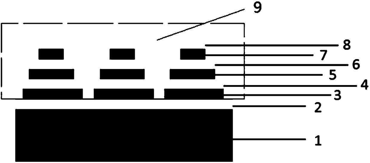
[0047] The metal film layer 1 is made of titanium and has a thickness of 200 nanometers, and the material of the dielectric film layer 2 is silicon dioxide and has a thickness of 30 nanometers.

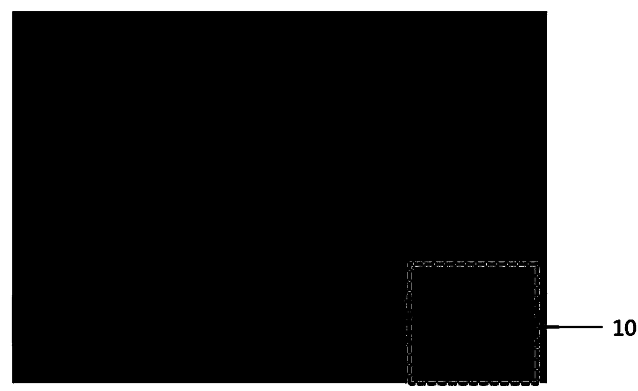
[0048] In the metal-medium composite structure 10, the diameters of the lower metal particle cylinder 3 and the lower medium particle cylinder 4 are consistent and are 200 nanometers, and the diameters of the middle metal particle cylinder 5 and the middle medium particle cylinder 6 are consistent and are 300 nanometers, The diameter of the upper metal particle column 7 is the same as that of the upper medium particle column 8 and is 400 nanometers.

[0049] The thickness of any layer of the cylindrical structure in the metal-dielectric composite structure 10 is 30 nanometers.

[0050] The lattice constant of the square periodic array composed of metal-dielectric composite structures 10 is 500 nanometers, that is, the horizontal di...

Embodiment 2

[0052] In another embodiment two of the present invention:

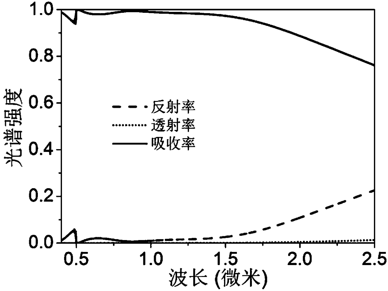
[0053] In this embodiment, on the basis of the first embodiment, the irradiation light is changed to the irradiation light of the standard solar light source AM1.5. attached Figure 4 It is the light absorption diagram of the perfect light absorber in the full spectrum range of solar energy of the present invention under the irradiation of standard solar light source AM1.5.

[0054] Reference attached Figure 4 , it can be found from the test spectrogram that under the irradiation of the standard solar light source AM1.5, the absorber produces an absorption spectral response that basically coincides with the spectral line of the standard light source. In the self-visible-infrared band from 280nm to 4000nm in the whole solar spectrum, the absorption spectral lines of the absorber basically repeat the spectral lines of the standard solar light source, with only a very slight intensity difference in the visible band. ...

Embodiment 3

[0055] In another embodiment three of the present invention:

[0056] In this embodiment, on the basis of the second embodiment, the light absorption diagram of the light absorption and loss comparison of the perfect light absorber in the full spectrum range of solar energy of this embodiment under the irradiation of the standard solar light source AM1.5 is measured.

[0057] Reference attached Figure 5 , the solid line is the spectral line of the solar spectrum absorbed by the absorber of the present invention under the irradiation of the standard solar light source AM1.5. The dotted line is the spectrum of the absorber that is not absorbed or lost under the illumination of this light source.

[0058] It can be found from the test spectrum that the absorber only has a very small part of the solar spectrum not absorbed in the visible band. In the entire solar spectrum range, the absorber provides an absorption efficiency as high as 0.972 relative to the irradiation intensit...


PUM

PropertyMeasurementUnit
Thicknessaaaaaaaaaa
Thicknessaaaaaaaaaa
Thicknessaaaaaaaaaa

Abstract

A visible-near infrared area broadband perfect absorber is featured by comprising a metal film, a medium film and a metal-medium stack layer; the metal-medium stack layer is arranged on the medium film; the medium film is arranged on the metal film; the metal-medium stack layer is formed by periodically arraying metal-medium composite structures. The solar energy full spectrum scope perfect lightabsorber has the high temperature and heat resistance physics property, thus effectively preventing metal ohmic losses, heat effect and thermal unstability problems, and realizing broadband absorptionof UV-visible-infrared wave bands; the electromagnetic wave in the solar energy full spectrum scope can be perfectly absorbed; the solar energy full spectrum scope perfect light absorber can be widely applied to the photoelectric devices under high temperature and heat resistance conditions, such as infrared detection and photoelectric conversion, infrared imaging, solar energy anti-reflection coating and heat radiator fields.

Description

technical field [0001] The invention relates to the field of photoelectric functional materials and devices and solar photovoltaic devices, in particular to a perfect light absorber in the full spectrum range of solar energy. Background technique [0002] Surface plasmon resonance (Surface Plasmon) usually refers to the collective oscillation caused by free electrons on the surface of a metal structure under the irradiation of external electromagnetic waves, forming a local electromagnetic field enhancement effect on the metal surface. [0003] Metamaterials refer to artificially designed and manufactured composite materials with periodic structures. In recent years, their research has rapidly become a frontier interdisciplinary field of physics, functional technology and material science. [0004] The concept of a perfect light absorber was first proposed in 2008 ("Physical Review Letters", Volume 100, Page 207402), which is a kind of electromagnetic wave plasmon resonance ...

Claims


Application Information

Patent Timeline
IPC IPC(8): G02B5/00
CPCG02B5/003G02B5/008
Inventor 刘正奇吴彪施雷雷刘桂强刘晓山
Owner JIANGXI NORMAL UNIV
Why Eureka
Try Eureka