Planar two-dimensional large-angle scanning antenna array

A technology for antenna arrays and scanning antennas, which is applied in the directions of antenna arrays, individually powered antenna arrays, and antennas. The effect of low lobe level, simple structure, and small gain fluctuation

Active Publication Date: 2018-10-16
XIDIAN UNIV
View PDF2 Cites 9 Cited by
  • Summary
  • Abstract
  • Description
  • Claims
  • Application Information

AI Technical Summary

Problems solved by technology

[0003] The invention provides a planar two-dimensional large-angle scanning antenna array, which is used to solve the technical problem that the microstrip patch antenna array in the prior art cannot perform two-dimensional large-angle scanning, and achieves simple structure and simple array arrangement. The technical effect of low side lobe level and small gain fluctuation during scanning

Method used


Image

  • Planar two-dimensional large-angle scanning antenna array
  • Planar two-dimensional large-angle scanning antenna array
  • Planar two-dimensional large-angle scanning antenna array

Examples


Embodiment 1

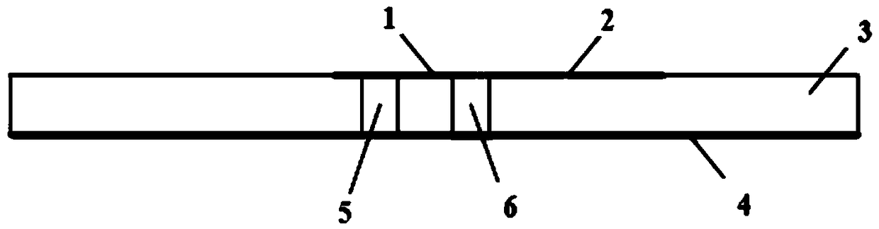
[0021] An embodiment of the present invention provides a planar two-dimensional large-angle scanning antenna array. The antenna array includes a first array and a second array, wherein the first array includes N complementary dipole antennas, and the second array includes N complementary dipole antennas. The array consists of M complementary dipole antennas, please refer to figure 1 , the complementary dipole antenna includes:

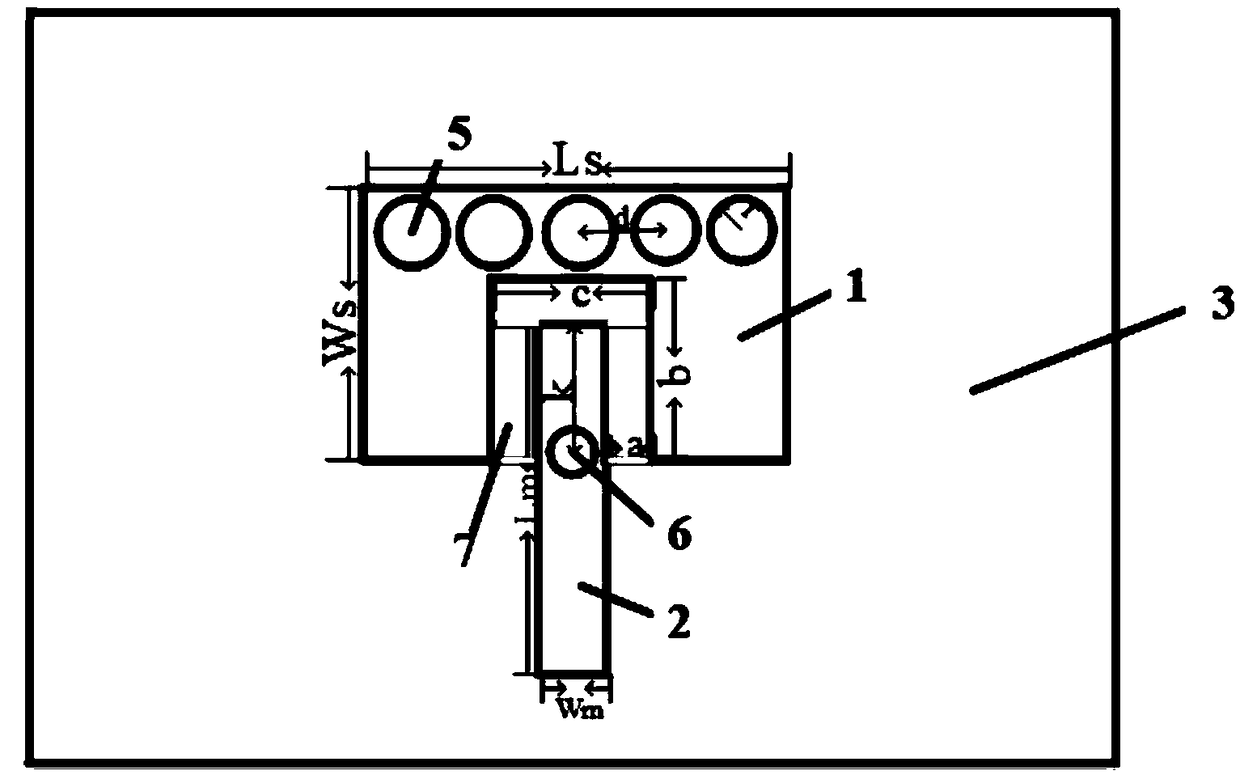
[0022] Dielectric substrate 3; the first microstrip patch 1, the first microstrip patch 1 is arranged on the upper surface of the dielectric substrate 3, wherein, the first microstrip patch 1 has a half opening groove 7;

[0023] Specifically, as figure 2 As shown, the dielectric substrate 3 adopts a relative permittivity of ε r , the thickness is h, its length and width are set to L and W respectively, the first microstrip patch 1 is arranged on the upper surface of the dielectric substrate 3, and the first microstrip patch 1 is a transverse micros...

Embodiment 2

[0038] A method for using a planar two-dimensional large-angle scanning antenna array of the present invention is described in detail below, specifically as follows:

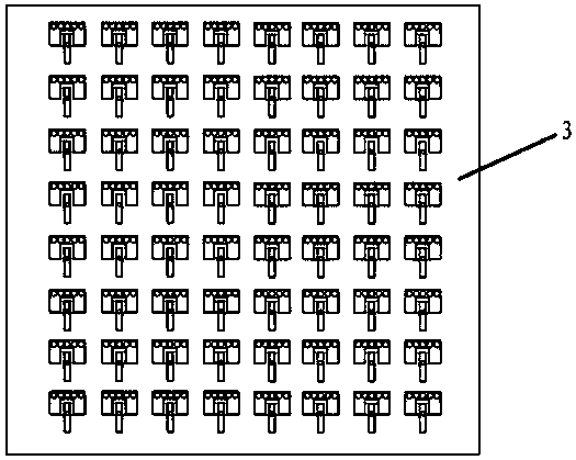
[0039] Take the 8*8 antenna array as an example, such as figure 1 As shown, the commercial electromagnetic simulation software HFSS is used to simulate and calculate the 8*8 antenna array, and the two-dimensional Cartesian coordinate pattern when the antenna array scans at different angles on the E plane can be obtained. At 70°~70°, the half-power beam width can cover the entire upper half space, and the sidelobe level is low during the whole scanning process. At the same time, the gain of the array can reach up to 21.6dB at the time of side-fire, and then with the increase of the scanning angle However, it gradually shows a downward trend, but generally speaking, the gain fluctuation of array scanning is basically controlled within the range of 3dB.

[0040] Furthermore, the two-dimensional Cartesian coordinat...


PUM


Abstract

The invention discloses a planar two-dimensional large-angle scanning antenna array, and relates to the technical field of antennas. The array antenna comprises a first array and a second array, wherein the first array comprises N complementary dipole antennas, the second array comprises M complementary dipole antennas, each complementary dipole antenna comprises a dielectric substrate, a first microstrip patch, a second microstrip patch, a floor, a coaxial feeder and P short-circuit metal posts, the first microstrip patch is arranged on an upper surface of the dielectric substrate, a half opening groove is formed in the first microstrip patch, the second microstrip patch is arranged on an upper surface of the dielectric substrate, the second microstrip patch is perpendicular to the firstmicrostrip patch, the floor is arranged at the bottom of the dielectric substrate, and the coaxial feeder is arranged in the dielectric substrate in a penetrating way. The technical effects of simplestructure, simple arraying mode, low side lobe level during the scanning process and small gain fluctuation are achieved.

Description

technical field [0001] The invention relates to the technical field of antennas, in particular to a plane two-dimensional large-angle scanning antenna array. Background technique [0002] The traditional microstrip antenna phased array is affected by the unit beam width and the mutual coupling between units, the scanning range of the main plane is generally -50°~50°, and the gain fluctuation can reach 4-5dB. When the array is arranged at equal intervals, grating lobes will appear in the visible area when the element spacing exceeds half a wavelength, and a large side lobe level will appear when the scanning angle is further expanded, which restricts the use of planar large-angle scanning phased arrays. application and development. The idea of ​​traditional large-angle scanning phased array antenna design is to use a microstrip patch antenna unit with a wide beam, and then realize the large-angle scanning of the array through an array at equal intervals, but most of the time...

Claims


Application Information

Patent Timeline
Patent Type & Authority Applications(China)
IPC IPC(8): H01Q1/38H01Q1/48H01Q1/50H01Q9/04H01Q21/06H01Q21/00
CPCH01Q1/38H01Q1/48H01Q1/50H01Q9/045H01Q9/0457H01Q21/0006H01Q21/065
Inventor 刘淑芳王府生史小卫张静雅李慧敏
Owner XIDIAN UNIV
Why Eureka
Try Eureka