
An infrared transparent window with electromagnetic shielding function

A transparent window, electromagnetic shielding technology, applied in the manufacture of circuits, electrical components, cables/conductors, etc., can solve the problems of reducing the electromagnetic shielding performance of materials, increasing the resistivity of materials, etc., to prevent the decrease of infrared transmittance and high electromagnetic shielding. , the effect of good application prospects

Active Publication Date: 2019-08-27
SUN YAT SEN UNIV
View PDF6 Cites 0 Cited by
  • Summary
  • Abstract
  • Description
  • Claims
  • Application Information

AI Technical Summary

Problems solved by technology

According to the Drude model, in order to extend the transmission window of traditional transparent conductive oxides to the mid-infrared band, it is necessary to reduce the free electron concentration or thickness of the material to reduce the reflection and absorption in the mid-infrared band, which often increases the resistivity of the material, Reduce the electromagnetic shielding performance of the material

Method used

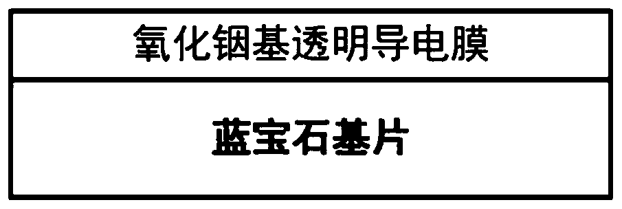

Image

  • An infrared transparent window with electromagnetic shielding function
  • An infrared transparent window with electromagnetic shielding function
  • An infrared transparent window with electromagnetic shielding function

Examples


Embodiment 1

[0036] Using existing MOCVD equipment, using organometallic trimethyl indium as the indium source, organometallic tetrakis(dimethylamino)tin as the doping source, oxygen with a purity of 99.9999% or more as the oxygen source, and argon with a purity of 99.999% or more as the source A protective atmosphere is grown to prepare an infrared transparent window.

[0037] The preparation method of the infrared transparent window of this embodiment is as follows:

[0038]1) Sapphire substrate pretreatment: A double-sided polished sapphire substrate with a thickness of 430 μm is selected as the main body of the infrared window, and there is a 0.2° deviation angle between the surface of the substrate and the sapphire c-crystal plane. After cleaning the surface of the sapphire substrate with organic and inorganic acid and alkali, put it into the MOCVD reaction chamber, control the temperature at 600° C., and control the pressure at 10 Torr for 30 minutes.

[0039] 2) Growth of indium ox...

Embodiment 2

[0045] The preparation method of the infrared transparent window of this embodiment is as follows:

[0046] 1) Sapphire substrate pretreatment: A double-sided polished sapphire substrate with a thickness of 430 μm is selected as the main body of the infrared window, and there is a 0.2° deviation angle between the surface of the substrate and the sapphire c-crystal plane. After cleaning the surface of the sapphire substrate with organic and inorganic acid and alkali, put it into the MOCVD reaction chamber, control the temperature at 600° C., and control the pressure at 10 Torr for 30 minutes.

[0047] 2) Growth of indium oxide-based transparent conductive film: the growth temperature is adjusted to maintain at 530° C., the pressure of the reaction chamber is controlled at 9 Torr, and argon gas is introduced as a protective atmosphere. The organometallic trimethylindium and oxygen were fed, and the flow rates were controlled at 6.0×10 -5 mol / min and 2.2×10 -2 mol / min, and dope...

Embodiment 3

[0050] The preparation method of the infrared transparent window of this embodiment is as follows:

[0051] Sapphire substrate pretreatment: A double-sided polished sapphire substrate with a thickness of 100 μm is selected as the main body of the infrared window, and the surface of the substrate has a 0° deviation angle from the sapphire c-crystal plane. After cleaning the surface of the sapphire substrate with organic and inorganic acid and alkali, put it into the MOCVD reaction chamber, control the temperature at 300° C., and control the pressure at 3 Torr for 60 minutes.

[0052] Indium oxide-based transparent conductive film growth: adjust the growth temperature to 400°C, control the reaction chamber pressure at 760Torr, and feed argon as a protective atmosphere. Introduce organometallic trimethyl indium and laughing gas, the flow rates are controlled at 6.0×10 -5 mol / min and 2.2×10 -2 mol / min, and doped with organometallic tetramethyltin, the flow control is the same as...


PUM

PropertyMeasurementUnit
thicknessaaaaaaaaaa
thicknessaaaaaaaaaa
thicknessaaaaaaaaaa

Abstract

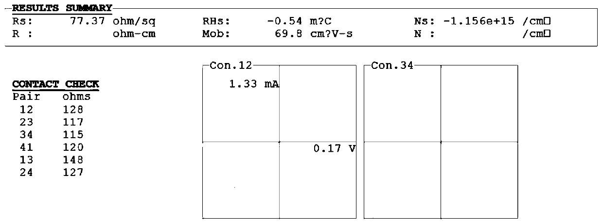
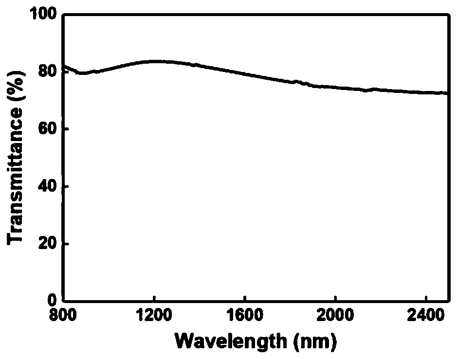
The invention provides an infrared transparent window with an electromagnetic shielding function. The infrared transparent window is composed of a sapphire substrate and an indium oxide-based transparent conductive film on the sapphire substrate. The square resistance of the infrared transparent window is lower than 100 omega / sq, the electron mobility is higher than 50 cm<2> / Vs, the transmittanceis averagely larger than or equal to 78% within the wavelength range of 0.78 micrometer to 2.5 mircrometer, and the transmittance is averagely larger than or equal to 68% within the wavelength range of 2.5 micrometers to 5 micrometers. The surface of the sapphire substrate and the crystal face c of a sapphire form a slip angle of 0 degree to 10 degrees, and the thickness ranges from 100 micrometers to 10,000 micrometers. According to the infrared transparent window, the indium oxide-based transparent conductive film is prepared through an MOCVD method, the transmittance within the near-infrared wave band of 0.78 micrometer to 2.5 micrometers and the intermediate-infrared wave band of 2.5 micrometers to 5 micrometers and the electromagnetic shielding performance can be considered at the same time, large-scale large-size production is convenient, and the infrared transparent window has good application prospects in the field of infrared photoelectric devices.

Description

technical field [0001] The invention belongs to the field of infrared optical materials and thin film materials, and mainly relates to an infrared transparent window with electromagnetic shielding function. Background technique [0002] Infrared technology, including infrared temperature measurement, infrared remote sensing, infrared imaging and infrared guidance, has important applications in civilian and even military fields. As a key component of the infrared detection / imaging system, the infrared transparent window needs to protect the infrared sensor and other optoelectronic devices from being damaged by the external environment on the one hand, and on the other hand, it must have good infrared transparency to ensure that the optical performance of the photoelectric sensor is not reduced . [0003] Sapphire crystal not only has good mechanical properties and chemical stability, but also has high transmittance in the mid-infrared 3-5 μm band, and is the main candidate m...

Claims


Application Information

Patent Timeline
Patent Type & Authority Patents(China)
IPC IPC(8): C23C16/40C23C16/44H01B5/14H01B13/00
Inventor 王钢卓毅陈梓敏
Owner SUN YAT SEN UNIV
Learn More