
Method for preparing wave absorbing material from copper slags, and wave absorbing material

A technology of wave absorbing material and copper slag, applied in the field of metallurgy, can solve the problems of less synthesis amount, easy agglomeration of wave absorbing materials, inability to mass-produce, etc., and achieves the effect of large synthesis amount and avoiding agglomeration

Active Publication Date: 2018-11-06
LANZHOU UNIVERSITY OF TECHNOLOGY
View PDF4 Cites 3 Cited by
  • Summary
  • Abstract
  • Description
  • Claims
  • Application Information

AI Technical Summary

Problems solved by technology

However, in the above preparation method, the wave-absorbing material is easy to agglomerate during the preparation process, and the amount of synthesis is small, so it cannot be mass-produced industrially.

Method used


Image

  • Method for preparing wave absorbing material from copper slags, and wave absorbing material
  • Method for preparing wave absorbing material from copper slags, and wave absorbing material
  • Method for preparing wave absorbing material from copper slags, and wave absorbing material

Examples


preparation example Construction

[0063] The present invention also provides the wave-absorbing material obtained by the above preparation method, the wave-absorbing material comprising the following raw materials in mass percentage:

[0064]

[0065] The particle size of the absorbing material is 70-150nm.

[0066] In the present invention, the particle size of the absorbing material is preferably 90-130 nm, more preferably 100-120 nm.

Embodiment 1

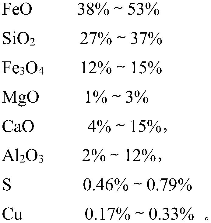
[0069] Copper slag is flash furnace copper slag, and its specific composition is:

[0070]

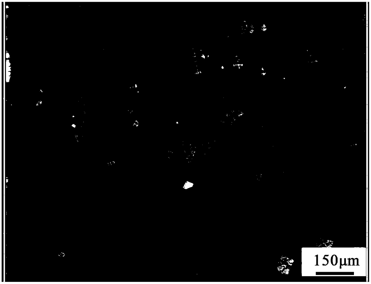
[0071] After crushing the copper slag, use a 200-mesh sieve (figure 1 Shown), the average particle size is 21 μm. The oxidized and modified copper slag is crushed to below 200 mesh, placed in a magnetic separator with a magnetic field strength of 100mT for magnetic separation. Put the magnetic substance in a ball mill, add ethanol as a dispersant, and grind for 24 hours until Fe 3 o 4 The particle size of the nano crystal is 70nm-90nm, and the wave-absorbing material is prepared.

Embodiment 2

[0073] Copper slag is silver furnace copper slag, and its specific composition is:

[0074]

[0075]

[0076] After crushing the copper slag, use a 200-mesh sieve (3 o 4 The particle size of the nano crystal is 100nm-120nm, and the wave-absorbing material is prepared.


PUM

PropertyMeasurementUnit
particle sizeaaaaaaaaaa

Abstract

The invention provides a method for preparing a wave absorbing material from copper slags, and belongs to the technical field of metallurgy. The method comprises the following preparation steps: mixing copper slags with calcium oxide and then performing tabletting to obtain modified copper slags; performing melting-oxidation on the obtained modified copper slags to obtain oxidation modified copperslags, and separating out a non-full granular magnetite phase; performing crushing and magnetic separation on the oxidation modified copper slags in sequence to obtain a magnetic substance; and grinding the obtained magnetic substance to 70 to 150 nm to obtain the wave absorbing material. According to the method provided by the invention, the copper slags are treated by using the melting-oxidation method, so as to enable iron components in the copper slags to selectively enrich with the magnetite phase, and Fe3O4 nanocrystals are embedded in various oxides, and a small quantity of oxide SiO2with dielectric properties is left still after the magnetic separation, the agglomeration of Fe3O4 particles caused by magnetic properties can be avoided, the synthesis capacity is large, and the massproduction can be realized.

Description

technical field [0001] The invention relates to the technical field of metallurgy, in particular to a method for preparing a wave-absorbing material from copper slag and the wave-absorbing material. Background technique [0002] my country's copper metallurgical enterprises accumulate a large amount of copper slag every year. my country's copper slag is mainly pyro-smelting slag, in addition to a considerable amount of converter slag and wet copper leaching slag. A large amount of copper slag not only occupies land, but also pollutes the environment and causes a huge waste of resources. The typical composition of copper slag is FeO38%~53%, SiO 2 27%~37%, Fe 3 o 4 12%~15%, MgO 1%~3%, CaO 4%~15%, Al 2 o 3 2% to 12%, S 0.46% to 0.79%, Cu 0.17% to 0.33%. It can be seen that the average TFe content in copper slag can reach more than 40%. If the iron resources in copper slag can be effectively developed and utilized, it will have an important impact on promoting the sustain...

Claims


Application Information

Patent Timeline
Patent Type & Authority Applications(China)
IPC IPC(8): C09K3/00H05K9/00
CPCC09K3/00H05K9/0081
Inventor 申莹莹黄仔牛杜雪岩种峻楷颜鹏泽张文娟
Owner LANZHOU UNIVERSITY OF TECHNOLOGY
Learn More