
A kind of idt copper process manufacturing method of tc-saw

A TC-SAW and manufacturing method technology, applied in the direction of impedance network, electrical components, etc., can solve the problems that the exposure and stripping process cannot be completed, the electrode shape is difficult to control, cumbersome and complicated, etc., and achieve easy to achieve, small insertion loss, and process simple effect

Active Publication Date: 2022-06-28
XIAMEN SANAN INTEGRATED CIRCUIT
View PDF6 Cites 0 Cited by
  • Summary
  • Abstract
  • Description
  • Claims
  • Application Information

AI Technical Summary

Problems solved by technology

However, due to the limitations of negative photoresist and stripping process, when the IDT electrode line width is less than 0.35 μm, the exposure and stripping process cannot be completed basically, and the shape of the electrode is difficult to control, which limits the use of TC-SAW products in the high frequency field. Applications
[0004] In high-frequency applications, BAW (bulk acoustic wave) technology is currently mainly used, and BAW technology requires more than a dozen photolithography processes, which is cumbersome and complicated, and the cost is high

Method used


Image

  • A kind of idt copper process manufacturing method of tc-saw

Examples


Embodiment Construction

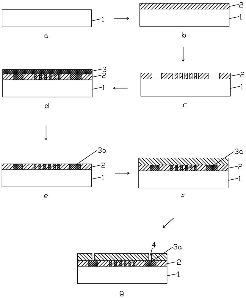
[0027] Combine the following figure 1 The process flow diagram of the IDT copper process manufacturing method of the TC-SAW of the present invention is shown to specifically illustrate the present invention.

[0028] Referring to 1a, a piezoelectric material substrate 1 is provided, which may be, for example, a lithium tantalate or a lithium tantalate-on-silicon crystal or the like.

[0029] refer to figure 1 b, depositing a dielectric material on the substrate 1 to form a first dielectric layer 2 . Dielectric materials include SiO 2 , Si 3 N 4 , Si x N y etc., deposited by methods such as CVD / PVD. The thickness of the first dielectric layer 2 ranges from 100 to 500 nm, for example, the reference is 200 nm. The thickness of the first dielectric layer 2 defines the thickness of the IDT metal, which can be adjusted according to product design requirements.

[0030] refer to figure 1 c. Coat positive photoresist, define the IDT pattern after exposure and development, an...


PUM

PropertyMeasurementUnit
thicknessaaaaaaaaaa
widthaaaaaaaaaa

Abstract

The invention discloses a TC-SAW IDT copper process manufacturing method, the steps of which are: forming a first dielectric layer on a piezoelectric substrate, and forming a first dielectric layer on the first dielectric layer through positive photoresist exposure and dry etching IDT graphic morphology, depositing the IDT metal layer, and then using the CMP process to grind the IDT metal layer to form a corresponding IDT metal structure, and then depositing the second dielectric layer. The present invention can effectively realize metal patterning and control of IDT metal morphology through positive photoresist combined with dry etching and CMP process, meet the requirements of smaller line width IDT electrodes, make the target frequency easier to achieve, and the process is simple , strong controllability, greatly reducing the cost.

Description

technical field [0001] The invention relates to the technical field of manufacturing surface acoustic wave filters, in particular to a method for manufacturing a TC-SAW IDT copper process. Background technique [0002] Surface Acoustic Wave (SAW) filters are widely used in signal receiver front ends as well as in duplexers and receive filters. The SAW filter combines low insertion loss with good rejection, enabling wide bandwidth and small size. In conventional SAW filters, the electrical input signal is converted into acoustic waves by intervening metallic interdigital transducers (IDTs), which are formed on a piezoelectric substrate. Among them, the temperature compensation filter (TC-SAW) is not easily affected by temperature changes, has more stable performance, and is more widely used. [0003] When the IDT structure of the existing TC-SAW filter is fabricated, a lift-off process (LIFT-OFF) is generally used, that is, a negative photoresist is used on the substrate to...

Claims


Application Information

Patent Timeline
Patent Type & Authority Patents(China)
IPC IPC(8): H03H3/02
CPCH03H3/02H03H2003/023
Inventor 邹福松杨濬哲尚荣耀朱庆芳谢祥政蔡文必
Owner XIAMEN SANAN INTEGRATED CIRCUIT
Learn More