MEMS SOI wafer and preparation method, and MEMS sensor and preparation method

A manufacturing method and wafer technology, applied in the field of MEMS sensors, can solve the problems of film thickness deviation, unusable wafers, MEMS membrane structure rupture, etc., to avoid film rupture and fragmentation, improve local stress concentration, and overcome film thickness deviation. Effect

Pending Publication Date: 2018-11-13
SUZHOU NOVOSENSE MICROELECTRONICS
View PDF0 Cites 2 Cited by
  • Summary
  • Abstract
  • Description
  • Claims
  • Application Information

AI Technical Summary

Problems solved by technology

For thicker MEMS film structures, the C-SOI process performs very well; but for thinner MEMS film structures (such as less than 10um), it is really dwarfed by the main reasons: first, in thinning, During the polishing process, as the thickness of C-SOI decreases, the MEMS membrane structure will be bent and deformed under the action of atmospheric pressure, which will not only cause the deviation of the membrane thickness, but also cause local stress concentration on the MEMS membrane structure, which is serious and directly Cause the membrane structure to break or even fragment; Second, in the subsequent manufacturing process, due to the thin film thickness and local stress, when the MEMS membrane structure undergoes standard cleaning and drying in the process, high-pressure water flow and air flow can easily cause The MEMS film structure breaks or even fragments of the MEMS C-SOI wafer; third, due to the problem of local stress, the MEMS device made of the thinner MEMS film structure has poor long-term stability and is easily affected by the external environment. Testing and use bring a lot of inconvenience; fourth, for ultra-thin film structures (below 5um), it is necessary to use more expensive SOI wafers to bond with ordinary silicon wafers, which is costly, complicated, and difficult to implement; fifth, In the preparation of C-SOI wafers, the dielectric layer is grown on the substrate or grown on the substrate and the device layer at the same time, and the film structure and support structure of the C-SOI wafer will bulge around, which will affect the roughness of the SOI wafer. , it will cause the wafer to be unusable in severe cases

Method used


Image

  • MEMS SOI wafer and preparation method, and MEMS sensor and preparation method
  • MEMS SOI wafer and preparation method, and MEMS sensor and preparation method
  • MEMS SOI wafer and preparation method, and MEMS sensor and preparation method

Examples


preparation example Construction

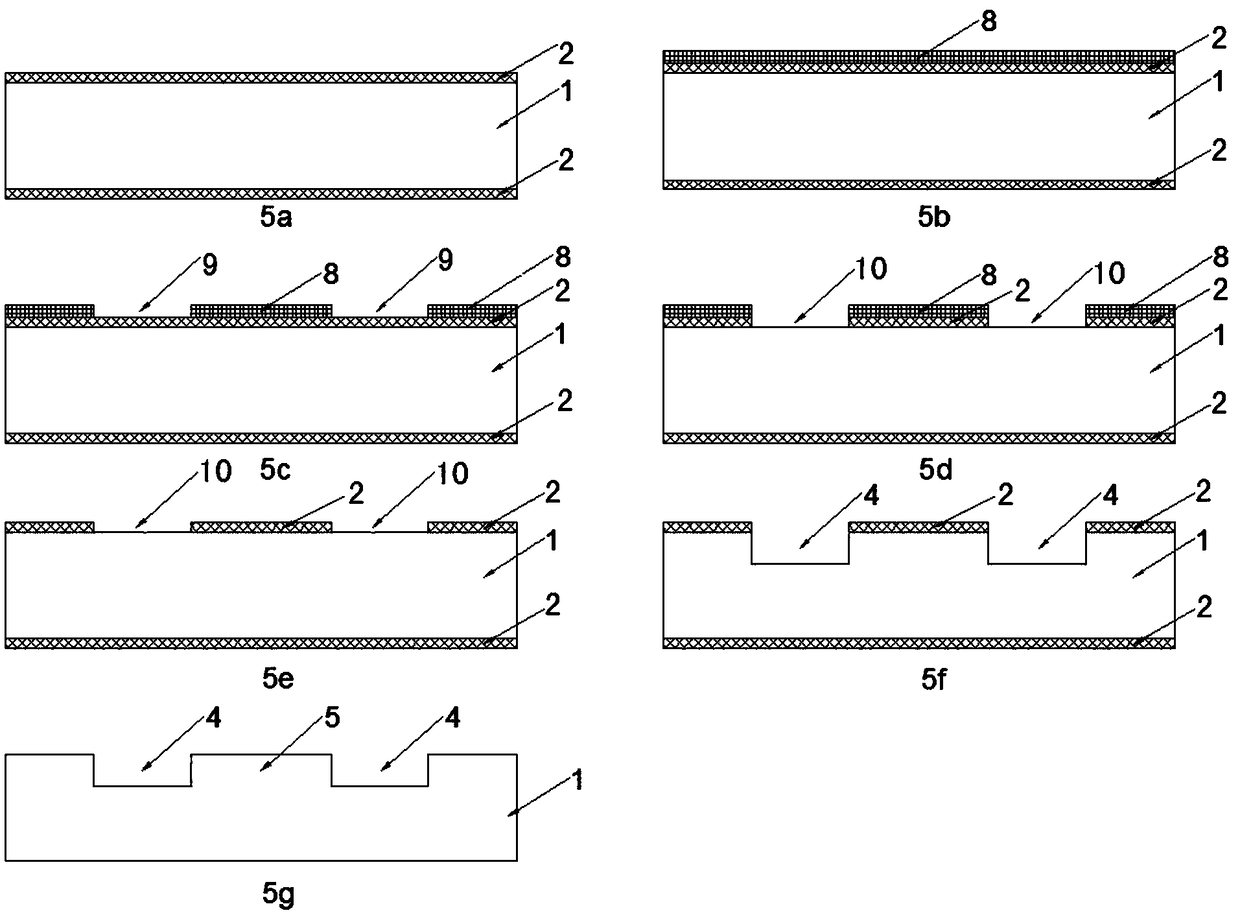
[0061] Such as Figure 5 Shown, the present invention discloses a kind of preparation method of MEMS SOI wafer, comprises the following steps:

[0062] (a) Preparation of the substrate 1: the commonly used semiconductor wafer is cleaned by a standard semiconductor process and then set aside;

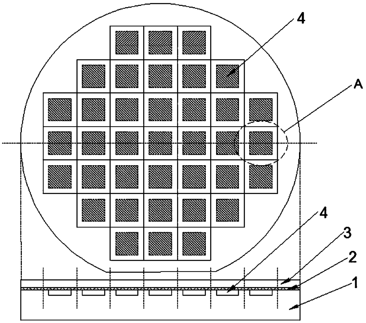
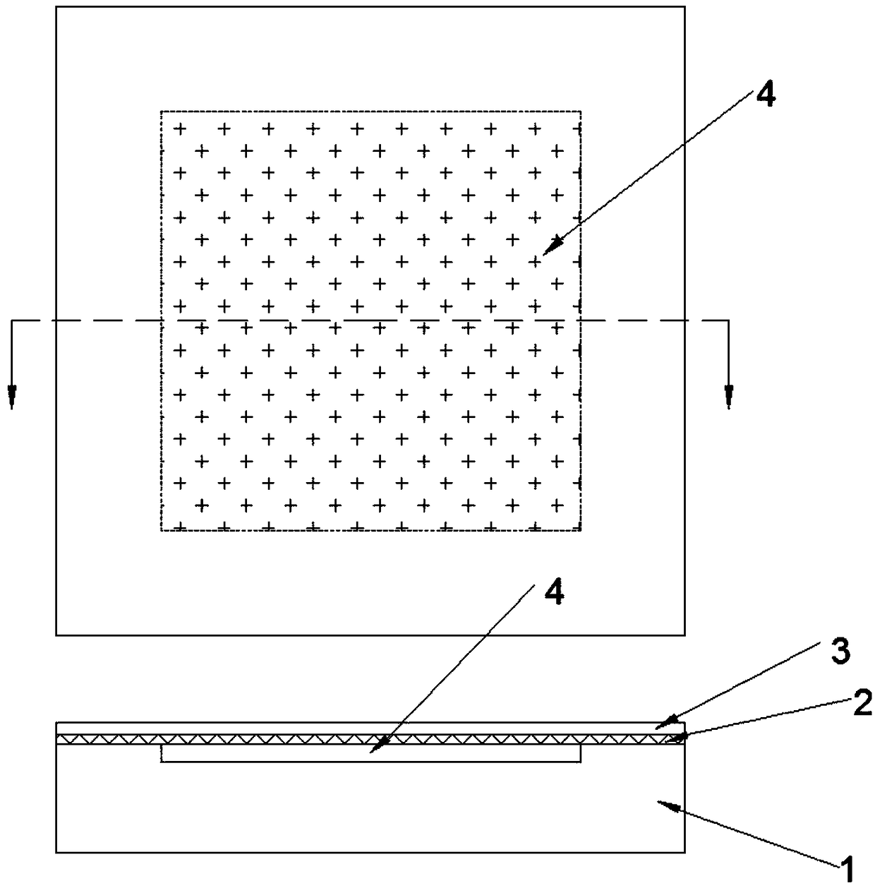
[0063] (b) Fabrication of grooves on the substrate: on the substrate 1, grooves and support structures 5 are formed by dry etching or wet etching, and the grooves are cavities 4;

[0064] (c) Preparation of the device layer wafer 6: select a conventional semiconductor wafer, such as an N-type (100) silicon wafer;

[0065] (d) Fabrication of the dielectric layer 2 on the device layer wafer 6: a layer of dielectric layer 2 is grown on the device layer wafer 6 by thermal oxidation or chemical vapor deposition to form a device layer wafer with a dielectric layer 2 on both sides 6;

[0066] (e) Bonding of the device layer wafer 6 to the substrate 1: the device layer wafer 6 with the dielec...

Embodiment 1

[0070] There are three methods for making grooves on the substrate in step (b), one of which is as Image 6 shown, including:

[0071] (4a) Spin-coat a layer of photoresist 8 on the substrate 1, bake and solidify, as a mask layer for dry etching the substrate 1;

[0072] (4b) Photoetching and developing the opening 9 of the dry-etched substrate;

[0073] (4c) dry etching the substrate from the opening 9 to form grooves and support structures;

[0074] (4d) Removing the photoresist to form a substrate 1 with grooves (ie cavities 4 ) and support structures 5 .

Embodiment 2

[0076] The second manufacturing method of the groove on the substrate in step (b) is as follows: Figure 7 shown, including:

[0077] (5a) growing a dielectric layer 2 on the substrate 1 by thermal oxidation or chemical vapor deposition as a mask layer for dry etching the substrate;

[0078] (5b) The substrate 1 with the dielectric layer 2 is spin-coated with a layer of photoresist 8, and baked and cured;

[0079] (5c) Photoetching and developing the opening 9 of the dielectric layer 2 by dry etching or wet etching;

[0080] (5d) etching away the dielectric layer 2 at the opening 9 by wet etching or dry etching to form the second opening 10 of the substrate 1 by dry etching;

[0081] (5e) removing photoresist 8;

[0082] (5f) dry etching the substrate 1 from the second opening to form a groove (ie cavity 4) and a supporting structure 5;

[0083] (5g) Wet etching the dielectric layer 2 on the substrate 1 to form the substrate 1 with grooves (ie cavities 4 ) and support stru...


PUM


Abstract

The invention discloses a MEMS SOI wafer and a preparation method, and a MEMS sensor and a preparation method thereof. The wafer structure comprises a substrate, a dielectric layer, a device layer anda cavity, wherein the cavity is located in the substrate, the cavity is formed with a support structure, the depth of the support structure is the same as the depth of the cavity, and the dielectriclayer is located between the substrate and the device layer. The preparation method comprises the following steps: preparation of a substrate; fabrication of a groove on the substrate; preparation ofa wafer on the device layer; fabrication of a dielectric layer on the wafer on the device layer; bonding of the wafer on the device layer to the substrate; and formation of a MEMS SOI wafer. The MEMSsensor fabricated by the wafer has the advantages of high practicability, excellent performance, good stability, and strong resistance to external environments.

Description

technical field [0001] The invention relates to a MEMS SOI wafer and a preparation method, a MEMS sensor using the MEMS SOI wafer and the preparation method and a preparation method thereof, and belongs to the technical field of MEMS sensors. Background technique [0002] MEMS membrane structure plays a pivotal role for MEMS sensors, especially MEMS pressure sensors. Early MEMS film structures are usually formed by traditional anisotropic wet etching in semiconductor technology, that is, using semiconductor materials, such as different crystal orientations of single crystal silicon, to have different etching rates in alkaline solutions. The disadvantages of this process are low efficiency, poor consistency, and low wafer utilization. With the advancement of semiconductor micromachining technology, silicon-on-insulator (Cavity-SOI, C-SOI) wafers with embedded cavities are increasingly used in the fabrication of MEMS sensors and gradually replace anisotropic Wet etching tech...

Claims


Application Information

Patent Timeline
IPC IPC(8): B81B1/00B81C1/00
CPCB81B1/00B81C1/00349B81C1/00373B81C1/00404
Inventor 桑新文盛云
Owner SUZHOU NOVOSENSE MICROELECTRONICS
Why Eureka
Try Eureka