

Optical detection device and detection method for hybrid integrated circuit component defects
A hybrid integrated circuit and defect optics technology, which is applied in the field of optical inspection, can solve problems such as poor welding and mounting of QFN package components, inability to detect, inconsistent amount of conductive adhesive, etc., so as to avoid inaccurate measurement of parameters and reduce false alarms and false positives, the effect of accurate solder ball radius
- Summary
- Abstract
- Description
- Claims
- Application Information
AI Technical Summary
Problems solved by technology
Method used
Image

Examples
Embodiment Construction
[0054] The embodiments of the present invention are described in detail below. This embodiment is implemented on the premise of the technical solution of the present invention, and detailed implementation methods and specific operating procedures are provided, but the protection scope of the present invention is not limited to the following implementation example.
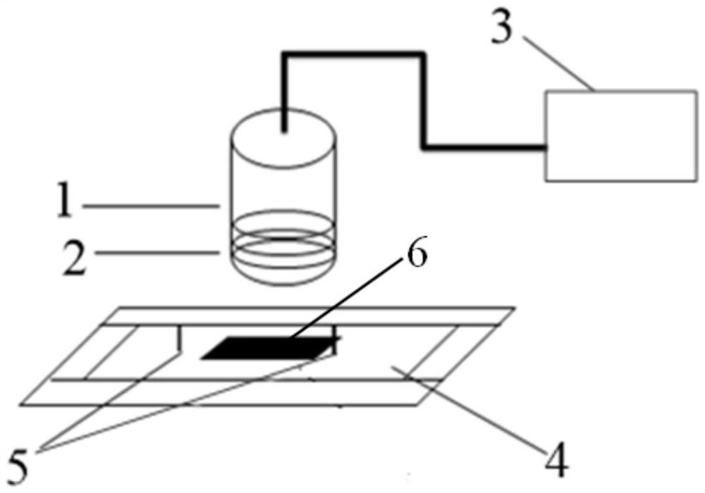
[0055] Such as figure 1 , the detection device of this embodiment includes a camera system 1 , an optical lighting system 2 , a computer system 3 , a conveying track 4 , a set of stoppers 5 and a component to be tested 6 .
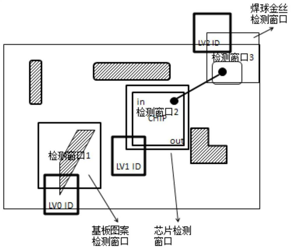
[0056] The set of stoppers 5 is located on the conveying track 4, and the component to be tested 6 is located between the set of stoppers 5. The component to be tested 6 contains substrates, chips, solder balls and other components to be tested. The optical lighting The system 2 is a ring-shaped LED light source, located directly above the component to be tested 6, the camera system 1 is locat...
PUM
 Abstract
Description
Claims
Application Information