A method for inspecting hot spots in photolithography process

A technology of photolithography process and inspection method, which is applied in microlithography exposure equipment, photolithography process of patterned surface, original parts for photomechanical processing, etc., can solve the problems of low efficiency and high cost of hot spot inspection of photolithography process , to achieve the effect of reducing inspection cost, reducing inspection scope and improving inspection efficiency

Active Publication Date: 2021-05-25
SHANGHAI HUALI MICROELECTRONICS CORP
View PDF2 Cites 0 Cited by
  • Summary
  • Abstract
  • Description
  • Claims
  • Application Information

AI Technical Summary

Problems solved by technology

[0004] The object of the present invention is to provide a method for inspecting hot spots in lithography process to solve the problem of high cost and low efficiency of hot spot inspection in existing lithography process

Method used


Image

  • A method for inspecting hot spots in photolithography process
  • A method for inspecting hot spots in photolithography process
  • A method for inspecting hot spots in photolithography process

Examples


Embodiment Construction

[0026] The method for inspecting hot spots in the photolithography process proposed by the present invention will be further described in detail below in conjunction with the accompanying drawings and specific embodiments. It should be noted that all the drawings are in a very simplified form and use imprecise scales, and are only used to facilitate and clearly assist the purpose of illustrating the embodiments of the present invention. In addition, the structures shown in the drawings are often a part of the actual structures. In particular, each drawing needs to display different emphases, and sometimes uses different scales.

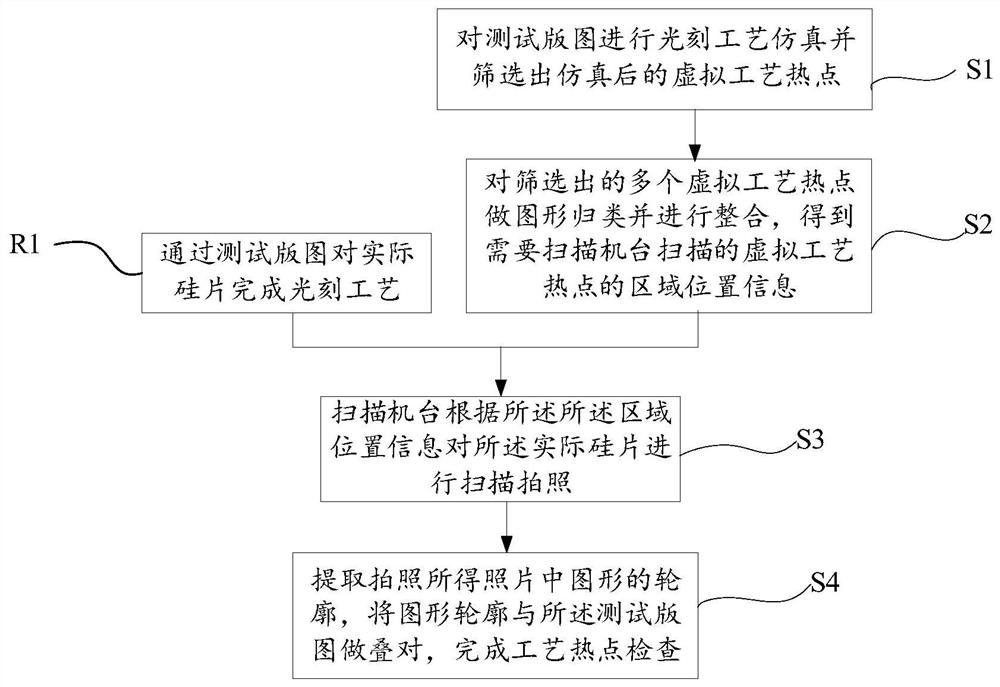
[0027] Such as figure 1 As shown, it is a flow chart of a method for inspecting hot spots in a photolithography process provided by an embodiment of the present invention, which includes four steps S1 to S4.

[0028] First, step S1 is performed, using the existing lithography simulation software (EDA) system to simulate the lithography process windo...


PUM


Abstract

The invention provides a method for checking hot spots of lithography process. The lithography process window is simulated and screened out by a lithography simulation software system to screen out the virtual process hotspots with a smaller window of the lithography process and screened out. Classify the obtained structures to obtain a virtual hotspot graphics library, scan the actual silicon chip that has been photolithographed through the test layout according to the location area of ​​each graphic in the virtual hotspot graphics library, and extract the actual structural graphics in the corresponding area The profile is compared with the test layout, and the hot spots of the actual lithography process are checked through the lithography simulation software system with reference to the test layout. By simulating the test layout and screening and categorizing the virtual process hotspots, the inspection scope of the actual process hotspots is greatly reduced, the inspection cost is reduced, and the inspection efficiency is improved.

Description

technical field [0001] The invention relates to the technical field of integrated circuit manufacturing technology, in particular to a method for checking hot spots in photolithography technology. Background technique [0002] In the integrated circuit manufacturing process, in order to smoothly transfer the pattern of the integrated circuit to the wafer, the mask plate is first made according to the designed layout, and then the pattern on the mask plate is transferred to the wafer by photolithography technology. superior. Due to the influence of the Optical Proximity Effect (OPE) in sub-wavelength lithography technology, large distortion will occur when exposing the highly densely arranged mask circuit pattern and finally transferring it to the wafer, such as Right-angled corner rounded, line end shortened, and line width increase / decrease are common reticle circuit patterns caused by the optical proximity effect. Defects transferred to the wafer. Although various resol...

Claims


Application Information

Patent Timeline
Patent Type & Authority Patents(China)
IPC IPC(8): G03F1/84G03F7/20
CPCG03F1/84G03F7/70616G03F7/7085
Inventor 朱忠华朱骏
Owner SHANGHAI HUALI MICROELECTRONICS CORP
Why Eureka
Try Eureka