A light guide component for a betavoltaic isotope battery
A technology of isotope batteries and light guide components, which is applied in the application of radiation from radioactive sources, obtaining electrical energy from radioactive sources, nuclear engineering, etc. The effect of energy conversion efficiency and electrical output power, increasing output efficiency, and efficient output
- Summary
- Abstract
- Description
- Claims
- Application Information
AI Technical Summary
Problems solved by technology
Method used
Image
Examples
Embodiment 1
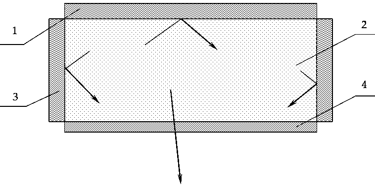
[0024] figure 1 It is a schematic diagram of the photoconductive assembly used in the radiovoltaic isotope battery of the present invention.
[0025] figure 1 Among them, the reflective film layer 1 and the side high reflective layer 3 are made of metal aluminum or silver, or low atomic number dielectric material SiO 2 , ZrO 2 Composed film system; luminescent material layer 2 is rigid luminescent material such as inorganic oxide, sulfide crystal and ceramics, or flexible organic luminescent material such as polyphenylene hydrocarbons, aromatic hydrocarbons and its derivatives, luminescent material The layer is in the form of flakes; the transmission film layer 4 is a single layer of SiO 2 , or multilayer dielectric material SiO 2 , ZrO 2 Composed of film systems, or multi-layer dielectric material SiO 2 、 Ta 2 o 5 Composed film system. The reflective film layer 1 is formed on the upper surface of the luminescent material layer 2 by electron beam evaporation or ion be...
Embodiment 2
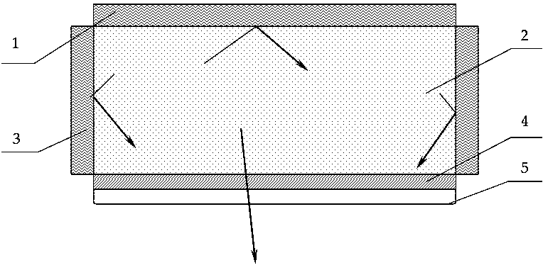
[0027] figure 2 It is a schematic diagram of a light guide component coated with silicone oil on the transmission surface.
[0028] figure 2 Among them, the reflective film layer 1 is formed on the upper surface of the luminescent material layer 2 by electron beam evaporation or ion beam sputtering, the side high reflection layer 3 is formed on the side of the luminescent material layer 2, and the transmissive film layer 4 is formed on the surface of the luminescent material layer 2. On the lower surface, a silicone oil layer 5 is coated on the surface of the transmissive film layer to couple the light guide component with the photovoltaic device.
Embodiment 3
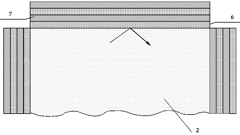
[0030] image 3 It is a multilayer dielectric material SiO 2 , ZrO 2 Schematic diagram of the combined film system.
[0031] image 3 Among them, the upper surface and side of the luminescent material layer 2 are plated with a multi-layer SiO26 and ZrO2 layer 7 by electron beam evaporation or ion beam sputtering, and by adjusting the number and thickness of the SiO2 layer 6 and ZrO2 layer 7, Realize 95% reflection of the light generated inside the luminescent material layer 2 on the upper surface and side surfaces.
PUM
| Property | Measurement | Unit |
|---|---|---|
| Thickness | aaaaa | aaaaa |
Abstract
Description
Claims
Application Information


