Image sensor and method for forming same

An image sensor and graphics technology, applied in the direction of electric solid-state devices, semiconductor devices, electrical components, etc., can solve the problems of small size, and achieve the effect of reduced usage, good controllability, and guaranteed performance

Inactive Publication Date: 2018-12-04
HUAIAN IMAGING DEVICE MFGR CORP
View PDF4 Cites 5 Cited by
  • Summary
  • Abstract
  • Description
  • Claims
  • Application Information

AI Technical Summary

Problems solved by technology

However, due to the limitation of photoresist performance, the current process method cannot achieve small size

Method used


Image

  • Image sensor and method for forming same
  • Image sensor and method for forming same
  • Image sensor and method for forming same

Examples


Embodiment Construction

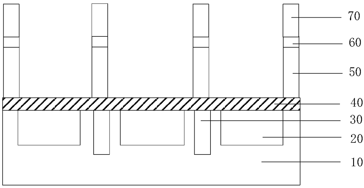
[0024] In the existing manufacturing process of the image sensor, in order to reduce the optical crosstalk of the incident light received by the image sensor device, it is necessary to form a metal grid on the surface of the semiconductor substrate.

[0025] Specifically, you can refer to figure 1 An image sensor formed by a prior art process is shown.

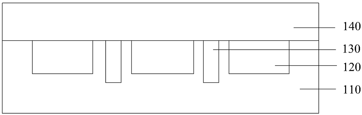
[0026] refer to figure 1 , a semiconductor substrate 10 is provided, and discrete photodiodes 20 are formed in the semiconductor substrate, and the discrete photodiodes 20 are isolated by deep trench isolation structures 30, and the deep trench isolation structures 30 The depth of the photodiode 20 is deeper than that of the photodiode 20, so as to obtain a better isolation effect and avoid the problem of diffusion of photo-generated carriers between different pixel regions.

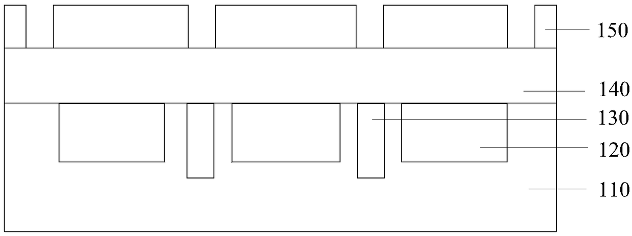
[0027] Then continue to refer to figure 1 , forming an interlayer dielectric layer 40 made of silicon oxide or silicon nitride or a combination of th...


PUM


Abstract

The technical solution of the present invention discloses an image sensor and a method for forming the same. The method for forming the image sensor includes: providing a semiconductor substrate; forming a first insulating layer on the semiconductor substrate; forming a patterned photoresist layer on the first insulating layer; by using the patterned photoresist layer as a mask, etching the firstinsulating layer to form a metal grid pattern; forming a second insulating layer on the sidewall and the bottom of the metal grid pattern; fully filling the metal grid pattern with a metal layer to form metal grids; and removing the second insulating layer outside the metal grids and a certain thickness of the first insulating layer. The method controls the critical dimension of the metal grids tomeet a corresponding requirement, and further ensures the performance of the image sensor and the yield of devices.

Description

technical field [0001] The invention relates to the field of manufacturing semiconductor devices, in particular to an image sensor and a forming method thereof. Background technique [0002] Image sensors receive light signals from objects and convert them into electrical signals that can be transmitted for further processing, such as digitization, and then stored in a storage device such as a memory, optical or magnetic disk, or for display on a display Display, print, etc. Image sensors are commonly used in devices such as digital cameras, video cameras, scanners, facsimile machines, and the like. [0003] Image sensors are generally of two types, Charge Coupled Device (CCD) sensors and CMOS Image Sensors (CMOS Image Sensors, CIS). Compared with CCD image sensors, CMOS image sensors have the advantages of high integration, low power consumption, and low production cost. [0004] At present, in the manufacturing process of CMOS image sensors, after the incident light is ...

Claims


Application Information

Patent Timeline
Patent Type & Authority Applications(China)
IPC IPC(8): H01L27/146
CPCH01L27/14623H01L27/14643H01L27/14685H01L27/14689
Inventor 孟俊生李志伟黄仁德
Owner HUAIAN IMAGING DEVICE MFGR CORP
Why Eureka
Try Eureka