Structure for reducing leakage in gallium nitride-based epitaxial layer and preparation method thereof

A gallium nitride-based, epitaxial layer technology, which is applied in the manufacture of circuits, electrical components, semiconductors/solid-state devices, etc., can solve problems such as large leakage current, poor reliability, and complicated production and preparation processes, and achieve short preparation cycles and reduce preparation costs. method, the effect of broad application prospects

Active Publication Date: 2018-12-07
PEKING UNIV +1
View PDF7 Cites 0 Cited by
  • Summary
  • Abstract
  • Description
  • Claims
  • Application Information

AI Technical Summary

Problems solved by technology

[0006] In view of the shortcomings of the prior art described above, the object of the present invention is to provide a structure and a preparation method for reducing leakage in gallium nitride-based epitaxial layers, by introducing an insertion layer between the upper...

Method used


Image

  • Structure for reducing leakage in gallium nitride-based epitaxial layer and preparation method thereof
  • Structure for reducing leakage in gallium nitride-based epitaxial layer and preparation method thereof
  • Structure for reducing leakage in gallium nitride-based epitaxial layer and preparation method thereof

Examples


preparation example Construction

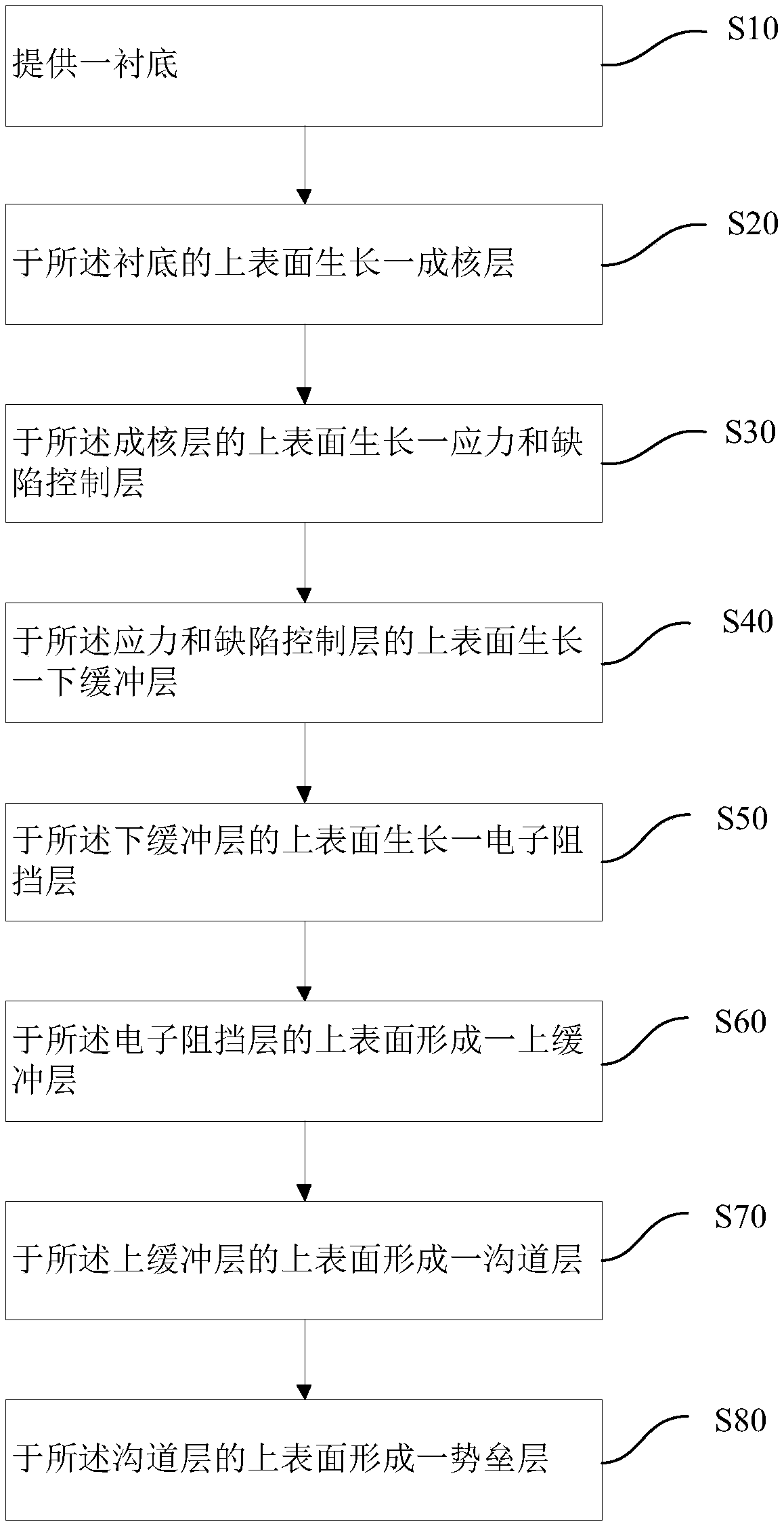
[0074] The present invention also provides a method for preparing the above-mentioned structure for reducing electric leakage in the gallium nitride-based epitaxial layer, such as figure 2 Shown, described preparation method comprises the following steps:

[0075] Step S10 is executed to provide a substrate 1, which may be a semiconductor substrate such as a silicon substrate or a silicon carbide substrate.

[0076] Executing step S20, growing a nucleation layer 2 on the upper surface of the substrate 1, the material of the nucleation layer 2 can be aluminum gallium nitride or aluminum nitride; the thickness of the nucleation layer 2 is 5nm-2μm , more preferably 20nm-1μm, more preferably 50nm-1μm.

[0077] Executing step S30, growing a stress and defect control layer 3 on the upper surface of the nucleation layer 2 for regulating the stress in the gallium nitride-based epitaxial layer and suppressing defects in the gallium nitride-based epitaxial layer The material of the s...

Embodiment 1

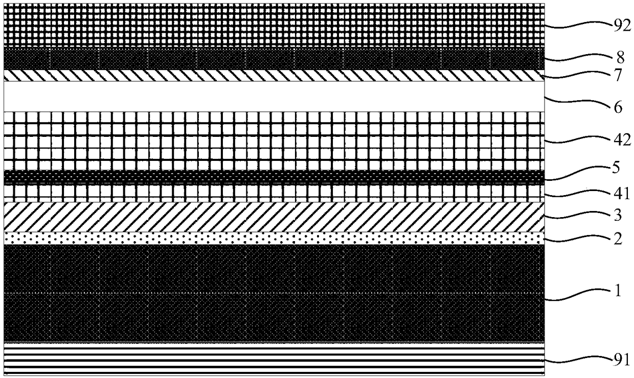
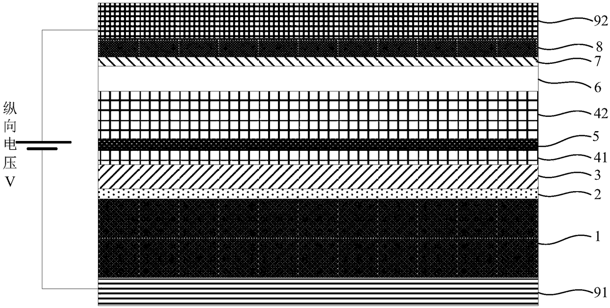
[0098] Preparation of a structure in which an electron blocking layer is introduced into a gallium nitride-based epitaxial layer: a silicon substrate is provided, and an aluminum nitride nucleation layer is sequentially grown upward on the surface of the silicon substrate by an epitaxial method, and AlGaN stress and defect control layer, GaN lower buffer layer, AlN electron blocking layer, GaN upper buffer layer, GaN channel layer, AlN insertion layer and AlGaN barrier layer; wherein, the AlN The thickness of the nucleation layer is 180nm-220nm, the thickness of the aluminum gallium nitrogen stress and defect control layer is 580-620nm, the thickness of the gallium nitride buffer layer (upper buffer layer+lower buffer layer) is 2450-2550nm, The thickness of the aluminum nitride electron blocking layer is 3-5nm, the thickness of the gallium nitride channel layer is 290-310nm, the thickness of the aluminum nitride insertion layer is 0.5nm-2nm, the aluminum gallium nitride potenti...


PUM

PropertyMeasurementUnit
Thicknessaaaaaaaaaa
Thicknessaaaaaaaaaa
Thicknessaaaaaaaaaa

Abstract

The invention provides a structure for reducing leakage in a gallium nitride-based epitaxial layer and a preparation method thereof. The structure for reducing leakage in the gallium nitride-based epitaxial layer prepared by an epitaxial method includes: a substrate; a nucleation layer, disposed on an upper surface of the substrate; a stress and defect control layer disposed on the upper surface of the nucleation layer; a lower buffer layer disposed on the upper surface of the stress and defect control layer; an electron blocking layer disposed on the upper surface of the lower buffer layer; an upper buffer layer disposed on the upper surface of the electron blocking layer; a channel layer disposed on the upper surface of the upper buffer layer; and a barrier layer disposed on the upper surface of the channel layer. By using the structure, the electron blocking layer is introduced in the upper buffer layer and the lower buffer layer, the barrier property of the electron blocking layercan be utilized to effectively block injection of electrons into the upper buffer layer, thereby effectively reducing the longitudinal leakage current in the gallium nitride-based epitaxial layer andimproving the reliability of the gallium nitride-based epitaxial layer.

Description

technical field [0001] The invention relates to the technical field of semiconductors, in particular to a structure for reducing electric leakage in gallium nitride-based epitaxial layers and a preparation method thereof. Background technique [0002] The third-generation semiconductors represented by group III nitrides have excellent properties such as high band gap, high breakdown electric field, high saturation electron drift velocity, and strong polarization, especially based on silicon (Si) substrates and silicon carbide ( Aluminum gallium nitride / gallium nitride (AlGaN / GaN) heterostructure high mobility transistor (HEMT) on SiC substrate has excellent characteristics such as fast switching speed, low on-resistance, small device size, high temperature resistance, and energy saving. , is expected to be widely used in the field of next-generation high-efficiency and energy-saving power electronic devices, including microwave radio frequency power devices and power electro...

Claims


Application Information

Patent Timeline
IPC IPC(8): H01L29/10H01L29/778H01L21/335
CPCH01L29/1075H01L29/66462H01L29/7786
Inventor 杨学林沈波宋春燕纪攀峰唐军齐胜利潘尧波
Owner PEKING UNIV
Why Eureka
Try Eureka