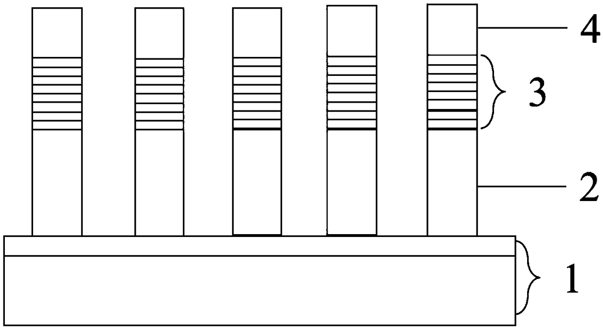
InGaN/GaN multiple quantum well nano-pillar grown on silicon/graphene composite substrate and preparation method thereof
A graphene composite, multi-quantum well technology, applied in semiconductor/solid-state device fabrication, phonon exciter, active region structure, etc., can solve the limitation of Si substrate LED development, large lattice mismatch thermal mismatch and other problems, to achieve the effect of convenient fabrication of vertical devices, improved crystal quality, and small value of half-peak width.
- Summary
- Abstract
- Description
- Claims
- Application Information
AI Technical Summary
Problems solved by technology
Method used
Image
Examples
Embodiment 1
[0037] The preparation method of the InGaN / GaN multi-quantum well nano-column grown on the Si / graphene composite substrate of the present embodiment comprises the following steps:
[0038] (1) Selection of the substrate and its crystal orientation: the substrate used is Si(111), polished on one side, and the thickness is 400±20μm;
[0039] (2) Substrate surface cleaning treatment: first, in carbon tetrachloride, toluene, acetone, absolute ethanol, respectively clean 3 times successively, each cleaning 3 minutes, remove the organic pollutant of Si substrate surface, use after Rinse with deionized water for 3 times; secondly, in the newly prepared H 2 SO 4 :H 2 o 2 (mass ratio is 1:1) in the solution for 3 minutes and then rinsed with 70°C deionized water for 3 times; finally, in HF:H 2 O (mass ratio: 1:10) solution was etched for 3 minutes, rinsed with deionized water and dried with high-purity dry nitrogen.
[0040] (3) Preparation of Si / graphene composite substrate: cut ...
Embodiment 2
[0047] The preparation method of the InGaN / GaN multi-quantum well nano-column grown on the Si / graphene composite substrate of the present embodiment comprises the following steps:
[0048] (1) Selection of the substrate and its crystal orientation: the substrate used is Si(111), polished on one side, and the thickness is 400±20μm;
[0049] (2) Substrate surface cleaning treatment: first, in carbon tetrachloride, toluene, acetone, absolute ethanol, respectively clean 3 times successively, each cleaning 3 minutes, remove the organic pollutant of Si substrate surface, use after Deionized water was ultrasonicated 3 times, 2 minutes each time; secondly, in the newly prepared H 2 SO 4 :H 2 o 2 (mass ratio is 1:1) in the solution for 3 minutes, then ultrasonicated 3 times with 70°C deionized water, 2 minutes each time; finally, in HF:H 2 O (mass ratio: 1:10) solution was etched for 3 minutes, and then deionized water was used to sonicate 3 times, 2 minutes each time, rinsed and d...
PUM
| Property | Measurement | Unit |
|---|---|---|
| height | aaaaa | aaaaa |
| height | aaaaa | aaaaa |
| thickness | aaaaa | aaaaa |
Abstract
Description
Claims
Application Information
 - R&D
- Intellectual Property
- Life Sciences
- Materials
- Tech Scout
- Unparalleled Data Quality
- Higher Quality Content
- 60% Fewer Hallucinations
Browse by: Latest US Patents, China's latest patents, Technical Efficacy Thesaurus, Application Domain, Technology Topic, Popular Technical Reports.
© 2025 PatSnap. All rights reserved.Legal|Privacy policy|Modern Slavery Act Transparency Statement|Sitemap|About US| Contact US: help@patsnap.com


