Light emitting assembly and light module

An optical emitting component and a technology for emitting light, applied in the field of optical communication, can solve the problems of module miniaturization and packaging, increase the loss of high-frequency signals, and affect the mass production of modules, so as to facilitate the implementation of the installation process, improve the yield, and reduce the impedance. The effect of discontinuity

Active Publication Date: 2018-12-18
LINKTEL TECH CO LTD
View PDF4 Cites 10 Cited by
  • Summary
  • Abstract
  • Description
  • Claims
  • Application Information

AI Technical Summary

Problems solved by technology

As the speed increases, the application of traditional packaging methods in the next generation of optical modules becomes difficult
[0004] From the perspective of signal yield, considering that with the progress of the times, the required rate is getting higher and higher, it is necessary to increase the number of light wave multiplexing, so that more LD chips need to be integrated in a miniaturized size, then It will inevitably cause too many devices in the housing, and those skilled in the art know that the more devices, the lower the yield rate of the processed optical signal will be, and such dense installation will also affect the implementation of the installation process, affecting Batch production of modules
[0005] From the perspective of signal quality, on the one hand, FPC generally has a longer length to accommodate assembly, and this length will cause more signal loss. On the other hand, FPC will introduce multiple impedance discontinuities such as welding pads. These discontinuities The point also significantly increases the high-frequency signal loss, and as the rate increases, the impact of this loss becomes greater and greater
[0006] From the structural point of view, in order to adapt to the design of welding FPC pads, the design should not be too small, resulting in the reserved pads on the PCB occupying a large amount of layout space. Also, as the module speed increases, the number of channels of the module will increase. This kind of space occupation will become more and more serious, making it difficult to miniaturize the package of the module

Method used


Image

  • Light emitting assembly and light module
  • Light emitting assembly and light module
  • Light emitting assembly and light module

Examples


Embodiment Construction

[0035] The following will clearly and completely describe the technical solutions in the embodiments of the present invention with reference to the accompanying drawings in the embodiments of the present invention. Obviously, the described embodiments are only some, not all, embodiments of the present invention. Based on the embodiments of the present invention, all other embodiments obtained by persons of ordinary skill in the art without making creative efforts belong to the protection scope of the present invention.

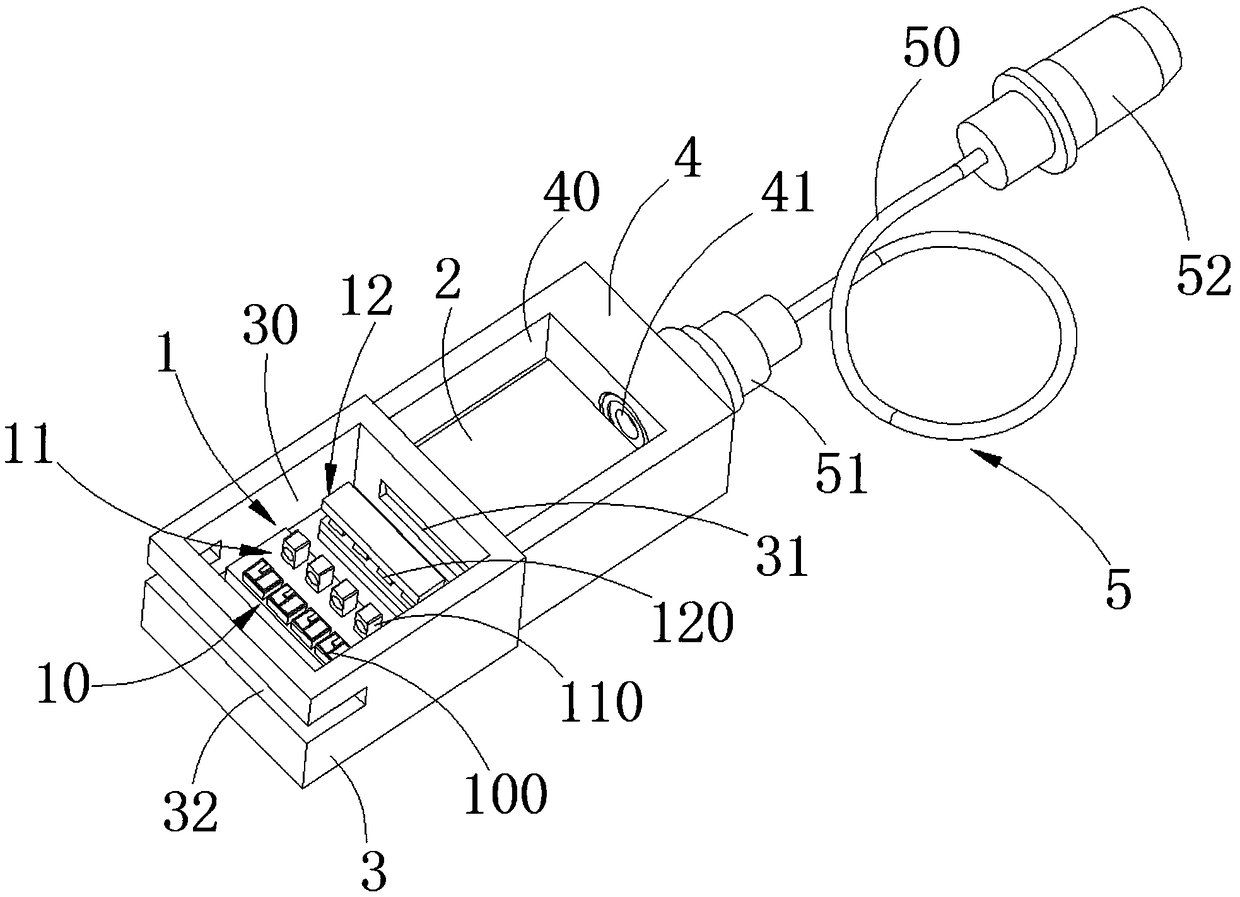
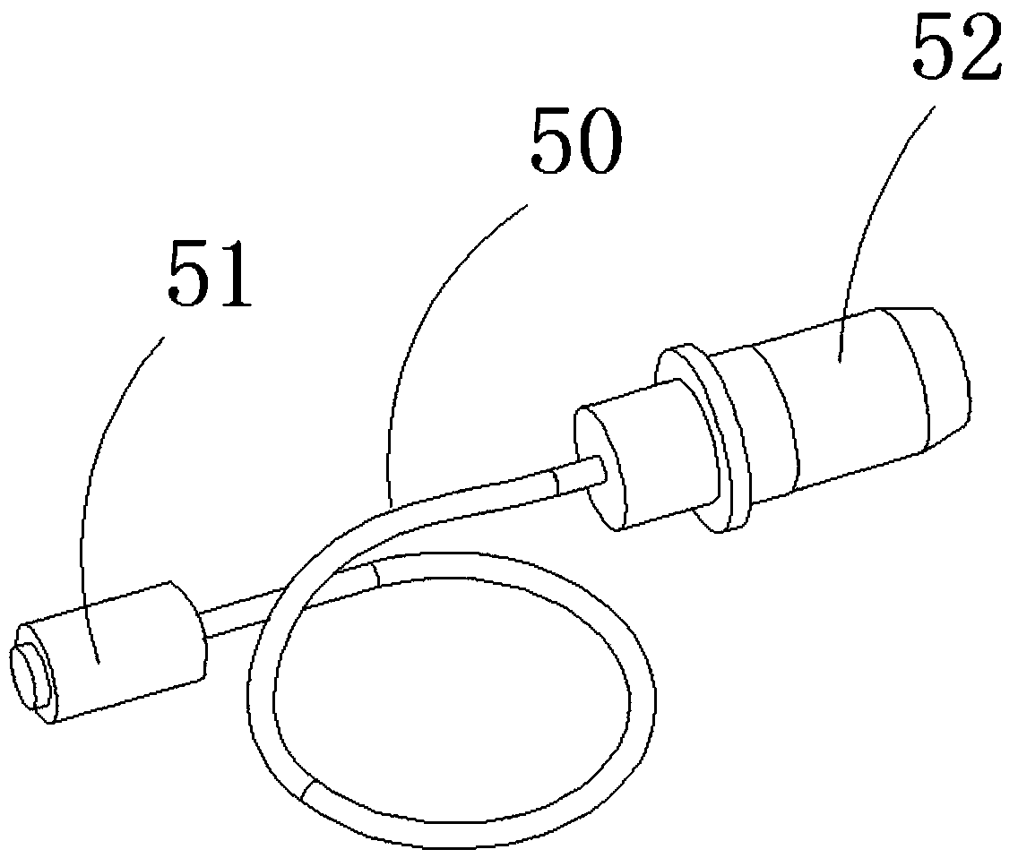
[0036] see figure 1 , an embodiment of the present invention provides a light emitting component, including an LD chip component 1 , an optical wavelength division multiplexer 2 , a first package 3 and a second package 4 . Wherein, the LD chip component 1 is used to transmit optical signals and optimize optical signals; the first package shell 3 is used to package the LD chip component 1; the optical wavelength division multiplexer 2 is used to receive the Th...


PUM


Abstract

The invention relates to the technical field of optical communication, and provides a light emitting assembly. The light emitting assembly comprises an LD chip component, an optical wavelength division multiplexer, a first packaging shell and a second packaging shell; the first packaging shell is fixedly connected with the second packaging shell, so as to form a first cavity for packaging the LD chip component and a second cavity for packaging the optical wavelength division multiplexer; the first cavity is located in the first packaging shell; and the second cavity is located in the second packaging shell. The invention further provides a light module. The light module comprises a shell, and further comprises a light receiving assembly and the light emitting assembly; and the light receiving assembly and the light emitting assembly are both arranged on the shell. The LD chip component and the optical wavelength division multiplexer are separated by adopting a two-section structure, and the processing of light signals is carried out in two steps, so that the yield is improved, and the implementation of the installation process is facilitated; and through the adoption of an opticalfiber adapter set, the assembly tolerance can be effectively compensated by utilizing the flexibility of optical fibers, the stress is eliminated, and the problem of light loss of the assembly due tothe stress is avoided.

Description

technical field [0001] The invention relates to the technical field of optical communication, in particular to an optical emitting component and an optical module. Background technique [0002] Higher speed, higher integration, and smaller package have always been the development direction of high-speed optical modules. At present, 100G QSFP28 optical transceiver modules with small package sizes have been applied in large quantities in data centers and Ethernet networks. The next generation of optical modules will be developed in the future. In a few years, it will be 200G, 400G, and then develop to 800G. In order to meet the high-density requirements of the optical interface of the optical switch, the package of 200G, 400G and even 800G optical modules must maintain the same size as QSFP28. A very high challenge. Among the four main components of the optical module, the light emitting component, the light receiving component, the PCB, and the packaging shell, the packaging...

Claims


Application Information

Patent Timeline
Patent Type & Authority Applications(China)
IPC IPC(8): G02B6/42
CPCG02B6/4256G02B6/4279G02B6/428G02B6/4285G02B6/4215G02B6/2938G02B6/293
Inventor 李林科林雪枫吴天书杨现文张健
Owner LINKTEL TECH CO LTD
Why Eureka
Try Eureka