A method for controllable preparation of organic semiconductor nanowire by synergistic action

An organic semiconductor, synergistic technology, applied in semiconductor devices, semiconductor/solid-state device manufacturing, nanotechnology for materials and surface science, etc. problem, to achieve the effect of simple, fast, high-quality, uniform dispersion, tailorable fluorescence quantum yield, and high fluorescence quantum yield

Active Publication Date: 2018-12-18
SUZHOU UNIV
View PDF1 Cites 5 Cited by
  • Summary
  • Abstract
  • Description
  • Claims
  • Application Information

AI Technical Summary

Problems solved by technology

However, both models have unavoidable deficiencies
The bottom-up mode requires additional processes to remove the template or additional electromagnetic field action; the top-down mode requires special conditions (high temperature, high voltage, etc.) Controllable Preparation of 100nm Organic Single Crystal Nanowires

Method used


Image

  • A method for controllable preparation of organic semiconductor nanowire by synergistic action
  • A method for controllable preparation of organic semiconductor nanowire by synergistic action
  • A method for controllable preparation of organic semiconductor nanowire by synergistic action

Examples


Embodiment 1

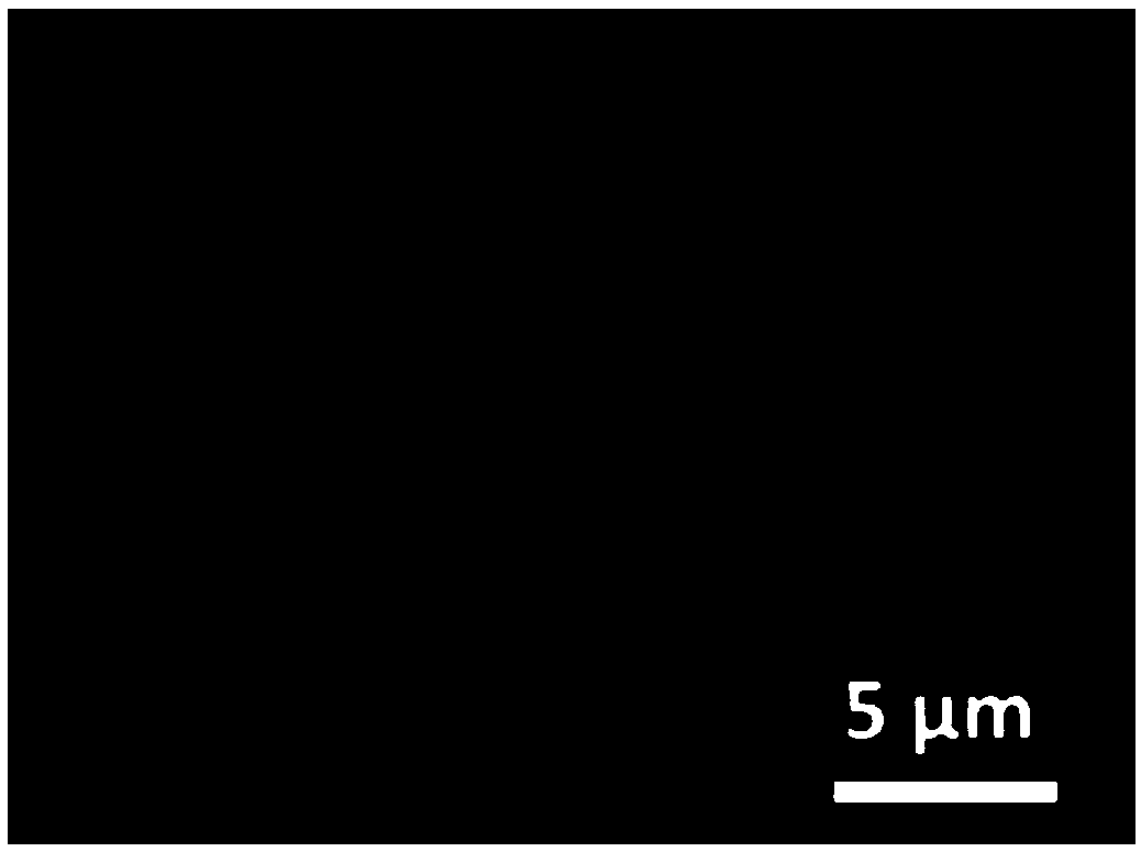
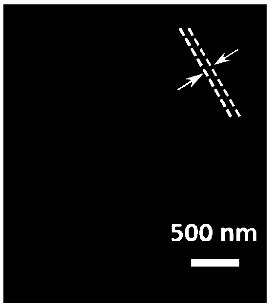
[0028] Add 6.97 mg of methoxydimethylaminoamine styryl phenyl ketone to 4 mL of dichloromethane and sonicate for 3 min to obtain a stock solution of methoxydimethylaminoamine styryl phenyl ketone dichloromethane. Take 1 mL of the stock solution and add it to 1 mL of ethanol, shake well, and then drop it on the substrate (such as silicon wafer, glass wafer or quartz wafer). After the organic solvent is evaporated to dryness, organic nanowires with a strong deep red color are obtained. By powder X-ray diffraction (XRD, Figure 4 ), scanning electron microscopy (SEM, Figure 5 ), transmission electron microscopy (TEM), and selected electron diffraction (SAED) ( Image 6 ) test means to characterize organic eutectic micro-crystals.

Embodiment 2

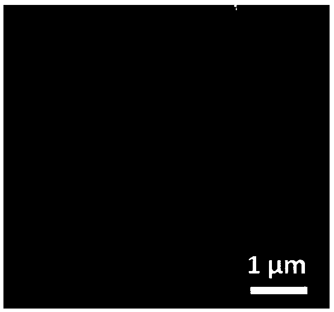
[0030] Add 6.35 mg of dimethylaniline styryl phenyl ketone to 4 mL of dichloromethane and sonicate for 3 min to obtain a stock solution of dimethyl aniline styryl phenyl ketone in dichloromethane. Take 1 mL of the stock solution and add it to 5 mL of ethanol to shake well, then drop it on the substrate, and obtain high-quality organic nanowires with uniform morphology after the organic solvent evaporates to dryness. scanning electron microscope (SEM, Figure 7 ) test means to characterize organic micro-crystals.

Embodiment 3

[0032] Add 6.94 mg of methoxydimethylaminoamine naphthalene vinyl phenyl ketone to 4 mL of dichloromethane and sonicate for 3 min to obtain a stock solution of methoxy dimethylaminoamine naphthyl vinyl phenyl ketone dichloromethane. Take 1 mL of the stock solution and add it to 10 mL of ethanol to shake well, then drop it on the substrate, and obtain high-quality organic nanowires with uniform morphology after the organic solvent evaporates to dryness. scanning electron microscope (SEM, Figure 8 ) test means to characterize organic micro-crystals.


PUM


Abstract

The invention provides a method for controllable synthesis preparation of organic semiconductor nanowire by synergistic action, includes accurately weighting organic semiconductor molecule, adding good organic solvent and ultrasonic wave to obtain organic semiconductor molecule organic solvent reserve solution, and At a certain volume ratio, that organic semiconductor molecule organic solvent reserve solution is added into an undesirable organic solvent to be shaken uniformly at room temperature, the organic semiconductor molecule reserve solution is dropped on the substrate aft standing for aperiod of time, and the organic solvent is evaporated and dried to obtain an organic single crystal nanowire structure material. The invention provides a new way for the preparation of simple, fast,controllable and uniform organic single crystal nanowires, and has very high academic value and application prospect in the development of nano-scale photoelectric devices.

Description

technical field [0001] The invention relates to a method for preparing an organic semiconductor nanowire material, in particular to a method for synergistically controlling the preparation of an organic semiconductor material nanowire. Background technique [0002] With the development of science and technology, the size of electronic devices is required to be further miniaturized, and the integration level of integrated circuits is further improved. However, traditional crafts encounter increasingly severe challenges in this respect. In the past two decades, one-dimensional nanowires, one of the most promising applications in nanoscale optoelectronic devices, have attracted more and more attention due to their unique physical and chemical properties. Because organic molecular materials are light in weight, cheap, flexible and tailorable, and have excellent optoelectronic properties and flexibility, organic semiconductor materials have certain advantages in optoelectronic d...

Claims


Application Information

Patent Timeline
Patent Type & Authority Applications(China)
IPC IPC(8): H01L51/00B82Y30/00B82Y40/00
CPCB82Y30/00B82Y40/00H10K71/10
Inventor 廖良生王雪东卓明鹏陶一辰李治洲
Owner SUZHOU UNIV
Why Eureka
Try Eureka