Semiconductor device
A semiconductor, conductive technology, applied in the direction of semiconductor devices, semiconductor/solid-state device manufacturing, transistors, etc.
- Summary
- Abstract
- Description
- Claims
- Application Information
AI Technical Summary
Problems solved by technology
Method used
Image
Examples
Embodiment approach 1
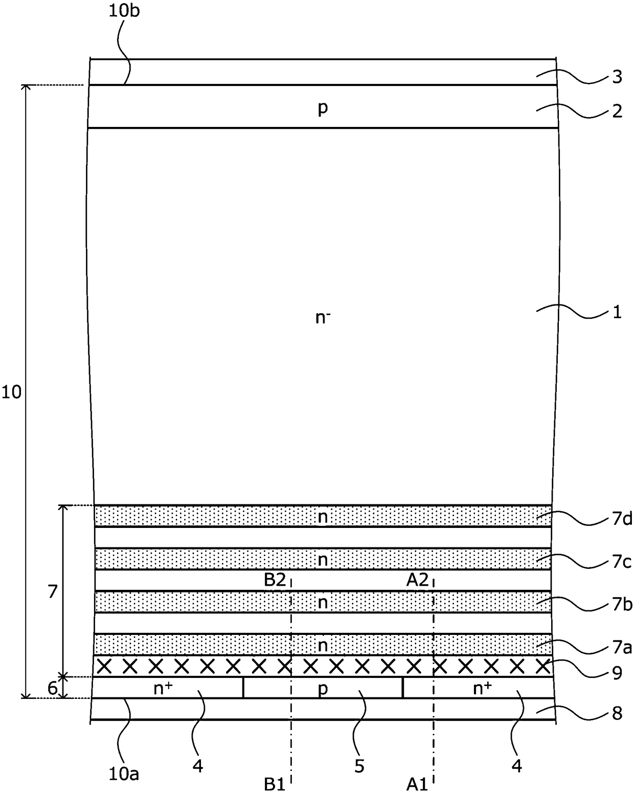
[0162] The structure of the semiconductor device according to Embodiment 1 will be described by taking a diode as an example. figure 1 is a cross-sectional view showing the structure of the semiconductor device according to the first embodiment. figure 1 The semiconductor device of Embodiment 1 shown is in n - The inside of the drift layer (first semiconductor layer) 1 is a diode including an n-type field stop layer (a plurality of n-type FS layers (first semiconductor regions) 7 ) having a plurality of peaks of impurity concentration in the depth direction. The depth direction is from n - The back side (second main surface) 10a of the type semiconductor substrate (semiconductor chip) 10 faces the direction of the front side (first main surface) 10b.
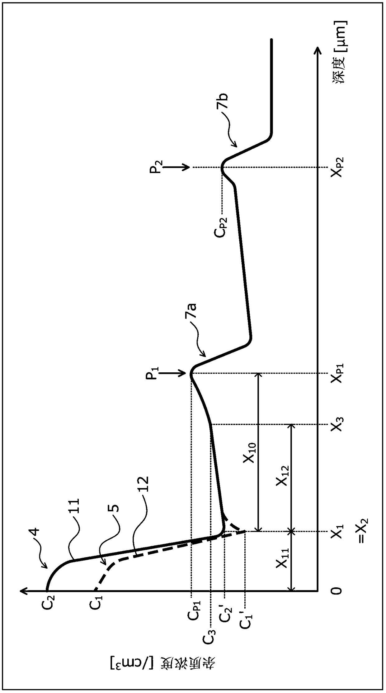
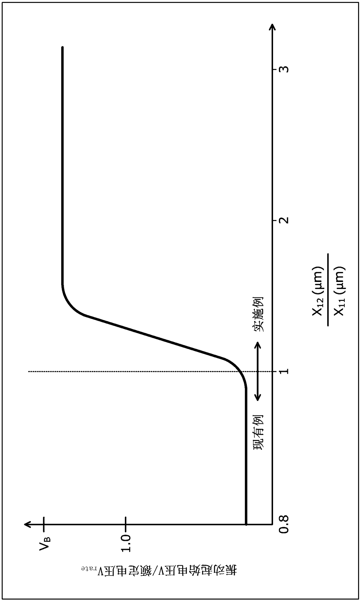
[0163] Specifically, a p-type anode layer (second semiconductor layer) 2 is provided on the surface layer of the front surface 10 b of the semiconductor substrate 10 . The p-type anode layer 2 is a diffusion region formed b...
Embodiment approach 2
[0199] Next, the structure of the semiconductor device according to Embodiment 2 will be described. Figure 10 is a cross-sectional view showing the configuration of a main part of the semiconductor device according to the second embodiment. exist Figure 10 2 shows the structure of the back surface 10a of the semiconductor substrate 10, and the illustration of the structure of the front surface 10b is omitted. In addition, as for the n-type FS layer 7, only the n-type FS layers 7a, 7b are shown (refer to figure 1 , figure 2 ) peak P of impurity concentration 1 ,P 2 . The difference between the semiconductor device of the second embodiment and the semiconductor device of the first embodiment is that, in the n constituting the cathode layer 6 + Type cathode region 4 and p-type cathode region 41, make the thickness X of p-type cathode region 41 11 than n + Thickness X of type cathode region 4 13 Thin.
[0200] The portion 52 of the n-type FS layer 7a opposite to the ...
Embodiment approach 3
[0206] Next, the structure of the semiconductor device of the third embodiment will be described. Figure 12 It is a cross-sectional view showing the structure of the main part of the semiconductor device according to the third embodiment. The semiconductor device according to the third embodiment differs from the semiconductor device according to the first embodiment in that an IGBT (Insulated Gate Bipolar Transistor: Insulated Gate Bipolar Transistor) and a diode are formed on the same semiconductor substrate 10 .
[0207] That is, the semiconductor device of Embodiment 3 is an RC-IGBT (Reverse Conducting-IGBT: Reverse Conducting IGBT) to which the FS structure of Embodiment 1 is applied. Specifically, after becoming n - On the same semiconductor substrate 10 as the drift layer 1 , an IGBT portion 61 in which an IGBT is disposed and an FWD portion 62 in which a FWD (Free Wheeling Diode: Free Wheeling Diode) is disposed are provided. The FWD of the FWD portion 62 is the sem...
PUM
| Property | Measurement | Unit |
|---|---|---|
| Thickness | aaaaa | aaaaa |
Abstract
Description
Claims
Application Information
 - R&D Engineer
- R&D Manager
- IP Professional
- Industry Leading Data Capabilities
- Powerful AI technology
- Patent DNA Extraction
Browse by: Latest US Patents, China's latest patents, Technical Efficacy Thesaurus, Application Domain, Technology Topic, Popular Technical Reports.
© 2024 PatSnap. All rights reserved.Legal|Privacy policy|Modern Slavery Act Transparency Statement|Sitemap|About US| Contact US: help@patsnap.com


