A method for fabricating n-MOSFET with composite double-layer epitaxy by boron implantation before epitaxy

A composite double-layer, epitaxial technology, applied in semiconductor/solid-state device manufacturing, electrical components, circuits, etc., can solve problems such as single particle burnout, affecting the normal operation of aerospace electronic equipment, and failure of power MOSFET devices, and achieves position and peak doping The impurity concentration is precisely controllable, and the effect of improving the secondary breakdown voltage and threshold current

Active Publication Date: 2018-12-25
BEIJING UNIV OF TECH
View PDF3 Cites 3 Cited by
  • Summary
  • Abstract
  • Description
  • Claims
  • Application Information

AI Technical Summary

Problems solved by technology

If the power MOSFET is in a blocking state during a collision transient, it may induce a single event burnout effect, resulting in failure of the power MOSFET device, thereby affecting the normal operation of the entire aerospace electronic equipment

Method used


Image

  • A method for fabricating n-MOSFET with composite double-layer epitaxy by boron implantation before epitaxy
  • A method for fabricating n-MOSFET with composite double-layer epitaxy by boron implantation before epitaxy
  • A method for fabricating n-MOSFET with composite double-layer epitaxy by boron implantation before epitaxy

Examples


preparation example Construction

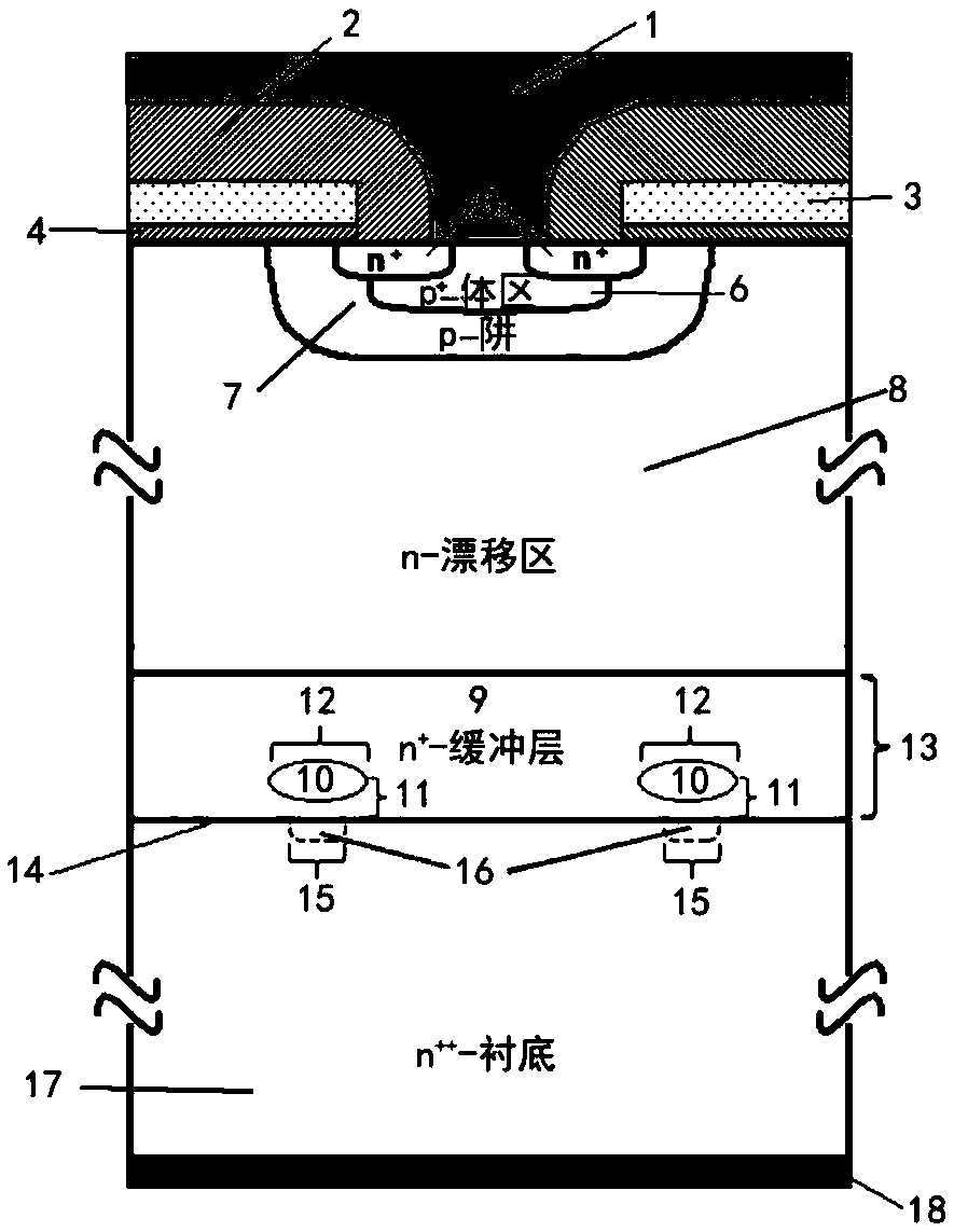
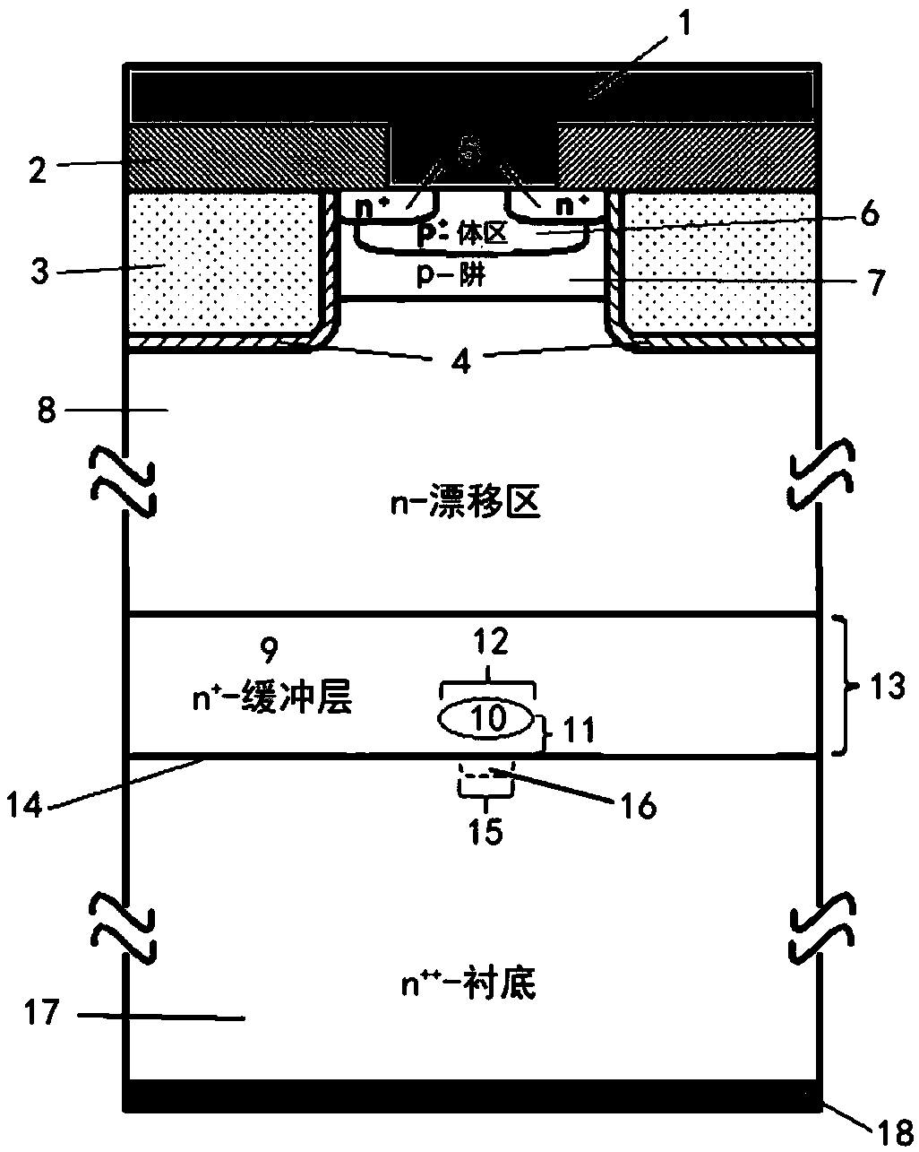
[0021] A kind of n-MOSFET preparation method of boron implantation composite double-layer epitaxy before epitaxy of the present invention comprises the following steps:

[0022] A) Select the substrate: the substrate is heavily doped n with (100) crystal orientation ++ type silicon substrate, the substrate is doped with arsenic or impurity;

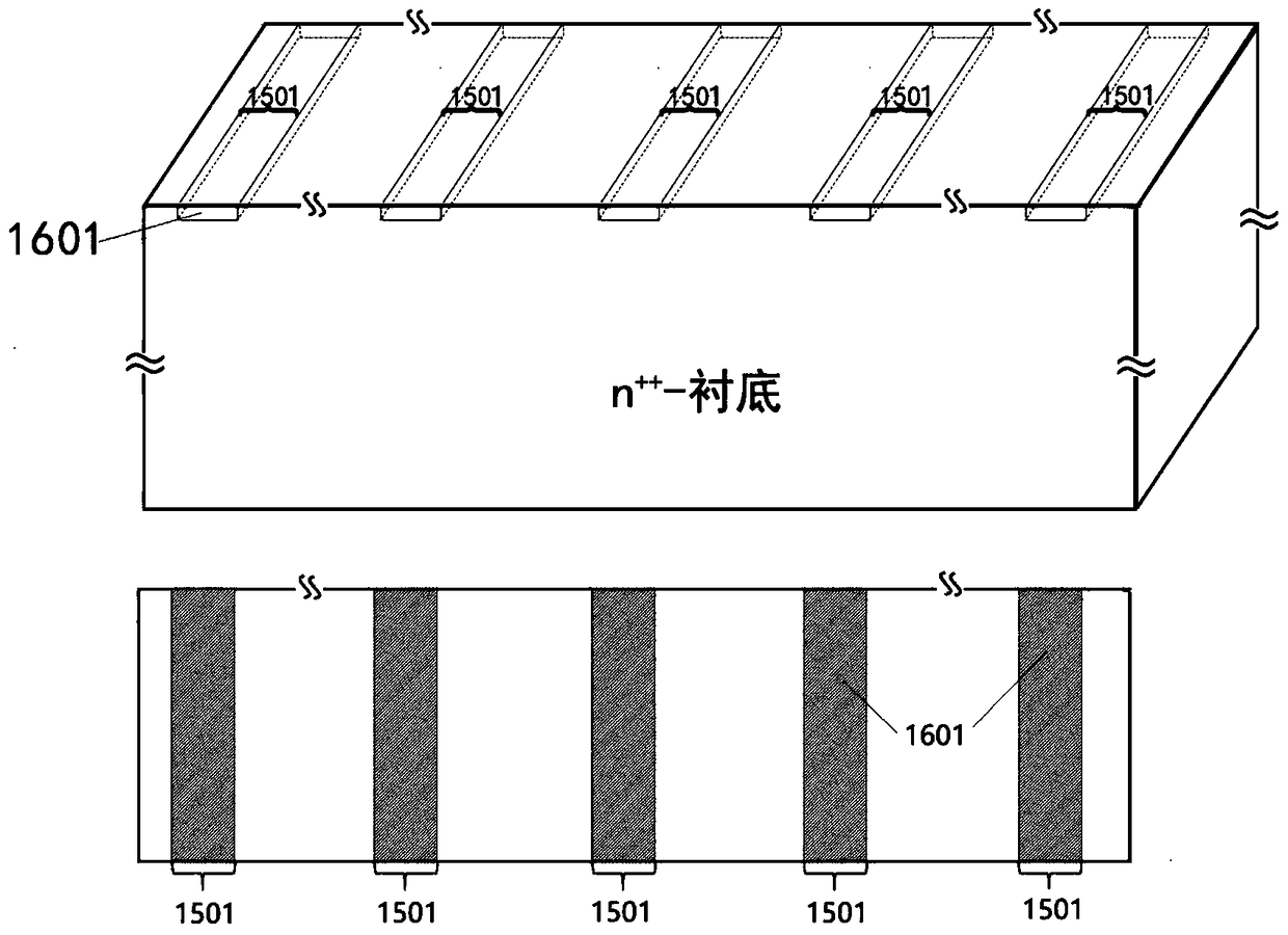
[0023] B) p-type island lithography: island lithography plate window and period control are the key to the process and one of the key points of the invention. The repetition period of the photolithographic window is exactly the same as that of the cell, and the shape is also consistent with the cell, which is strip (1601) or square (1602), and the window width (1501 or 1502) is 0.5 microns to 2 microns, as shown in Figure 3(a) , as shown in Figure 3(b).

[0024] C) P-type island boron tape glue injection: the dose of boron injection is also the key point of the invention, which is 1×10 13 cm -2 to 1×10 14 cm -2 Between, the injectio...

Embodiment 1

[0028] Example 1 Preparation of boron-implanted composite double-layer epitaxial planar gate MOSFET before epitaxy

[0029] This embodiment is a process for preparing a planar gate MOSFET with a p-type island buffer layer structure, with a withstand voltage of 200V. The specific process is as follows:

[0030] (1) On a (100) crystal orientation and arsenic-doped substrate with a resistivity of 0.01Ωcm, the photolithography and etching process of the plate marking is carried out;

[0031] (2) Island implantation photolithography, the photolithographic pattern is strip-shaped, the width of the strip is 0.7 microns, and the repetition period is 10 microns;

[0032] (3) p-type island implantation, implantation energy 80keV, dose 5×10 13 cm -2 ;

[0033] (4) Buffer layer epitaxy, buffer layer epitaxy doped with phosphorus, concentration 2×10 16 cm -3 , thickness 15 microns;

[0034] (5) Epitaxy in the drift region, the epitaxial layer is doped with phosphorus, and the doping...

Embodiment 2

[0037] Example 2 Preparation of boron-implanted composite double-layer epitaxial trench gate MOSFET before epitaxy

[0038] This embodiment is a process for preparing a planar gate MOSFET with a p-type island buffer layer structure, and the withstand voltage is 100V. The specific process is as follows:

[0039] (1) On a (100) crystal orientation and antimony-doped substrate with a resistivity of 0.02Ωcm, the photolithography and etching process of the plate marking is carried out;

[0040] (2) Island implantation photolithography, the photolithography pattern is a square, the side length is 1.5 microns, and the repetition period is 12 microns;

[0041](3) p-type island implantation, implantation energy 60keV, dose 3×10 13 cm -2 ;

[0042] (4) Buffer layer epitaxy, buffer layer epitaxy doped with phosphorus, concentration 5×10 16 cm -3 , with a thickness of 10 microns;

[0043] (5) Epitaxy in the drift region, the epitaxial layer is doped with phosphorus, and the doping ...


PUM

PropertyMeasurementUnit
thicknessaaaaaaaaaa
thicknessaaaaaaaaaa
thicknessaaaaaaaaaa

Abstract

The invention relates to a method for fabricating n-MOSFET with composite double-layer epitaxy by boron implantation before epitaxy which includes carry out p-type island photolithography and boron implantation before epitaxy process, and carrying out buffer lay epitaxy and voltage-resistant layer epitaxy after junction substrate material is selected and epitaxy process is carried out. The subsequent process is the same as that of conventional power MOSFETs. The implantation window size of p-type island and the implantation dose of boron are strictly controlled to ensure that the device is inunipolar mode when conducting. At that same time, when the device is in the blocking state, the p-type island pair buffer layer The electric field near the high and low junctions of the substrate canbe adjusted to improve the electric field distribution near the high and low junctions and to increase the single event burnout threshold of the device.

Description

technical field [0001] The invention belongs to the preparation technology of power semiconductor devices, and specifically relates to a method for preparing n-MOSFET by injecting boron before epitaxy and compound double-layer epitaxy. The device prepared by this technology has a certain anti-burning ability when irradiated by high-energy charged particles. Suitable for space work environments with single particle irradiation. Background technique [0002] Due to its superior performance such as fast switching speed and simple drive circuit, power MOSFETs are widely used in various electronic equipment for power conversion and processing such as rectification, inverter, boost, step-down, and frequency conversion. At the same time, with the excellent performance and mature technical advantages of the device, silicon-based power MOSFET is also considered to be one of the most satisfactory devices in the field of space electronic system applications, and is widely used in vario...

Claims


Application Information

Patent Timeline
Patent Type & Authority Applications(China)
IPC IPC(8): H01L21/336H01L29/06
CPCH01L29/0684H01L29/66666
Inventor 胡冬青张鹤泷贾云鹏吴郁唐伯晗唐蕴
Owner BEIJING UNIV OF TECH
Why Eureka
Try Eureka