A light emit diode

A technology of light-emitting diodes and metal electrodes, which is applied in the direction of electrical components, circuits, semiconductor devices, etc., and can solve the problem that the surface of the metal electrode of the LED core is easily corroded.

Active Publication Date: 2018-12-25
TIANJIN SANAN OPTOELECTRONICS
View PDF3 Cites 4 Cited by
  • Summary
  • Abstract
  • Description
  • Claims
  • Application Information

AI Technical Summary

Problems solved by technology

[0005] In view of the above-mentioned shortcomings of the prior art, the purpose of the present invention is to provide a light-emitting diode, which is used to solve the technical problem that the surface of the metal electrode of the LED core and the exposed part of the side are easily corroded in the prior art.

Method used


Image

  • A light emit diode
  • A light emit diode
  • A light emit diode

Examples


Embodiment 1

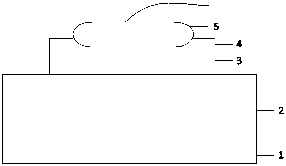
[0042] Such as figure 1 As shown, the light-emitting diode is a flip-chip red light-emitting diode, including from bottom to top: a back metal electrode and a conductive substrate 1, and the front side of the conductive substrate includes a multi-layer metal layer: a metal bonding layer, a metal reflective layer and a transparent Insulating layer (metal bonding layer, metal reflective layer and transparent insulating layer are not shown in the figure), wherein the transparent insulating layer is located on the metal reflective layer and is in front contact with the light-emitting epitaxial structure 2, and the transparent insulating layer includes through holes and fills them The metal conductive material is used for the metal reflective layer to form electrical contact with one side of the light-emitting epitaxial structure. The upper side of the light-emitting epitaxial structure includes a front electrode, and the surface of the front electrode is provided with a low-potent...

Embodiment 2

[0049] The difference from Example 1 is that the electrode pads at least include an ohmic contact layer, an anti-diffusion layer and a wire metal layer, the material of the ohmic contact layer is Cr, and the material of the anti-diffusion layer is Ti / Pt / Ni / W / TiW One of the metals that can block the diffusion between the solder layer and the ohmic contact layer; the ohmic contact layer is gold. The low-potential metal is one of Al, Zn, Cr, Ti, Fe, Co, and the low-potential metal layer is a compression-resistant metal material layer to improve the compressive strength of the electrode pad and slow down the welding line. For the pressure damage to the electrode pad during gold ball bonding, the Mohs hardness of the low-potential metal is preferably higher than 6, and more preferably the metal material is a metal material with high Mohs hardness such as Ti and Cr.

Embodiment 3

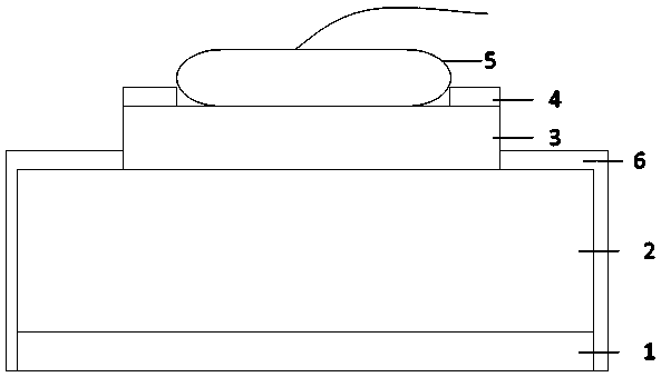
[0051] Different from embodiment 1 or 2, such as Figure 4 As shown, the insulating protection layer preferably further extends to the side surface and the outermost peripheral area of ​​the electrode pad, and at least partially covers the low-potential metal layer, and forms the middle of the pad electrode together with the low-potential metal layer and the insulating protection layer. Leave the area blank for wire bonding to gold balls for soldering, or if Figure 5 As shown, the insulating protection layer preferably exposes a part of the low-potential metal layer, so as to increase the protective effect of the low-potential metal on the surface of the metal layer of the electrode pad and wire. or as Image 6 As shown, the low-potential metal layer is located in the non-edge area, and the edge area is left blank for making an insulating protective layer covering.


PUM

PropertyMeasurementUnit
Mohs hardnessaaaaaaaaaa

Abstract

A light emit diode is characterized in that the light emit diode comprises a light emitting epitaxial structure; a metal electrode formed on the light emitting epitaxial structure and electrically connected to the light emitting epitaxial structure; at least a portion of the surface of the metal electrode is covered by a low-potential metal layer, and the potential of the metal used in the low-potential metal layer is lower than the potential of the metal on the surface side of the metal electrode. The low-potential metal layer can effectively solve the technical problem that the surface and the exposed part of the LED core metal electrode are easy to be corroded in the prior art.

Description

technical field [0001] The invention belongs to the field of semiconductor lighting, in particular to a light-emitting diode with a metal electrode protective layer. Background technique [0002] As a new type of high-efficiency solid light source, semiconductor lighting has significant advantages such as long life, energy saving, environmental protection, and safety. It will become another leap in the history of human lighting after incandescent lamps and fluorescent lamps. The upgrading of the industry and other industries has huge economic and social benefits. Because of this, semiconductor lighting is generally regarded as one of the most promising emerging industries in the 21st century, and also one of the most important commanding heights in the field of optoelectronics in the next few years. Light-emitting diodes LEDs are usually made of semiconductors such as GaN (gallium nitride), GaAs (gallium arsenide), GaP (gallium phosphide), GaAsP (gallium arsenide phosphide)...

Claims


Application Information

Patent Timeline
Patent Type & Authority Applications(China)
IPC IPC(8): H01L33/40H01L33/44
CPCH01L33/40H01L33/44
Inventor 蒙成吴俊毅王笃祥
Owner TIANJIN SANAN OPTOELECTRONICS
Why Eureka
Try Eureka