Method for improving etching uniformity of high aspect ratio tungsten alloy

A technology of tungsten alloy and photoresist, applied in metal material coating process, process for producing decorative surface effect, coating, etc.

Active Publication Date: 2019-01-01
PEKING UNIV
View PDF9 Cites 1 Cited by
  • Summary
  • Abstract
  • Description
  • Claims
  • Application Information

AI Technical Summary

Problems solved by technology

[0006] The purpose of the present invention is to provide a method for improving the etching uniformity of high aspect ratio tungsten alloys, which can keep the etc

Method used


Image

  • Method for improving etching uniformity of high aspect ratio tungsten alloy
  • Method for improving etching uniformity of high aspect ratio tungsten alloy
  • Method for improving etching uniformity of high aspect ratio tungsten alloy

Examples


Embodiment Construction

[0033] In order to make the above-mentioned features and advantages of the present invention more comprehensible, the following specific embodiments are described in detail in conjunction with the accompanying drawings.

[0034] In this embodiment, the method of the present invention is used to etch the tungsten-based alloy, and the steps are as follows:

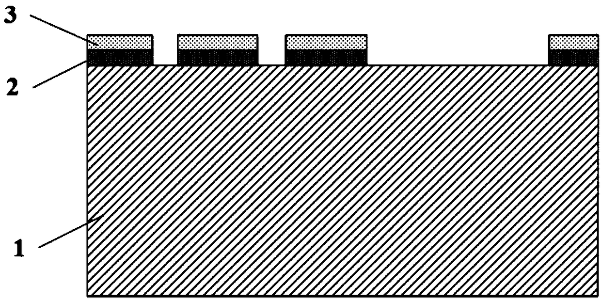
[0035] Step 1: Prepare hard mask layer pattern such as image 3 As shown, first, a layer of hard mask 2 (thickness 50nm-10μm) is deposited on a tungsten alloy substrate 1 (thickness 200μm-6mm) by sputtering, thermal evaporation and other methods. The tungsten alloy can be pure tungsten, tungsten carbide, tungsten-molybdenum alloy, tungsten-copper alloy, tungsten-rhenium alloy or hard alloy. The adhesion between the hard mask 2 and the tungsten alloy substrate 1 should be strong enough, commonly used are Al thin film, Ni thin film, Ti thin film and so on. Then, spin-coat the first layer of photoresist 3 on the surface of th...


PUM

PropertyMeasurementUnit
Thicknessaaaaaaaaaa
Thicknessaaaaaaaaaa

Abstract

The invention provides a method for improving the etching uniformity of a high aspect ratio tungsten alloy. The method comprises: growing a hard mask on a tungsten alloy substrate; carrying out spin coating of a first layer photoresist on the hard mask, and carrying out photoetching and developing to form a first layer photoresist pattern; etching the hard mask according to the first layer photoresist pattern to form a hard mask pattern; carrying out spin coating of a second layer photoresist, and carrying out photoetching and developing to form a second layer photoresist pattern; carrying outfirst tungsten alloy etching according to the second layer photoresist pattern, wherein the etching depth on the tungsten alloy substrate having a small opening area achieves a load effect amount; and removing the remaining second layer photoresist, and carrying out second tungsten alloy etching according to the hard mask pattern, such that the etching depth on the tungsten alloy substrate havinga small opening area and the etching depth on the tungsten alloy substrate having a large opening area are the same.

Description

technical field [0001] The invention belongs to the technical field of micro-electro-mechanical systems (MEMS), and in particular relates to a method for improving the etching uniformity of tungsten alloys with high aspect ratios. Background technique [0002] In the processing and manufacturing of MEMS devices, single crystal silicon materials are usually used as traditional structural substrate materials, and single crystal silicon materials have some inherent defects, such as high brittleness and poor impact resistance; compared with metal materials, their conductivity is poor, and their resistivity is relatively low. Higher; thermal stability is relatively poor, and Young's modulus will change significantly when it exceeds 600 ° C, which is not suitable for application under high temperature conditions, which affects the application range of the device. [0003] Metal tungsten material is the metal with the highest melting point in nature (3410°C), and it has the charact...

Claims


Application Information

Patent Timeline
IPC IPC(8): B81C1/00
CPCB81C1/00063B81C1/00404B81C1/00523
Inventor 陈兢李轩扬宋璐夏雁鸣
Owner PEKING UNIV
Why Eureka
Try Eureka