

SiCO separation layer material with low dielectric constant and preparation method thereof, and application of SiCO separation layer materials with low dielectric constant
A technology with low dielectric constant and dielectric constant, applied in the direction of metal material coating process, coating, circuit, etc., can solve the problems of poor tolerance, high dielectric constant, single composition, etc., and achieve good process parameters, Effect of reduced capacitive coupling and low dielectric constant
- Summary
- Abstract
- Description
- Claims
- Application Information
AI Technical Summary
Problems solved by technology
Method used
Image

Examples
Embodiment 1
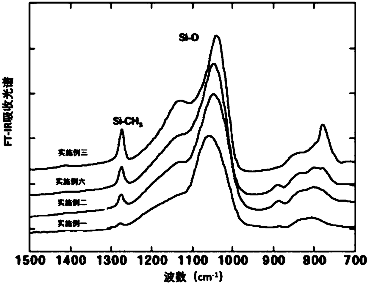
[0039] A low dielectric constant SiCO spacer film, based on CO / CO 2 The mixed gas is used as the oxidant, prepared by plasma-enhanced atomic layer deposition method, the film contains -Si-CH 3 structure. The dielectric constant of the film is 4, the C content is 5%, and the density is 2.3g / cm 3 , with 90% coverage.
[0040] A kind of preparation method of the SiCO spacer thin film of low dielectric constant, comprises the following steps:
[0041] 1) In the PEALD reaction chamber, heat a silicon wafer with a thickness of 525 μm and a diameter of 100 mm to 300 ° C;
[0042] 2) Using helium (He, introduction speed 100 sccm) as the carrier gas, diisopropylamine silane (DIPAS) was introduced into the reaction chamber as the first reactant at the introduction speed of 0.2 mg / min, and the introduction time was 0.1 second, and the reaction The air pressure in the chamber is maintained at 150Pa;
[0043] 3) Pump out the excess DIPAS, and purge with He gas for 10 sec at a purge ra...
Embodiment 2
[0048] A low dielectric constant SiCO spacer film, based on CO / CO 2 The mixed gas is used as the oxidant, prepared by plasma-enhanced atomic layer deposition method, the film contains -Si-CH 3 structure. The dielectric constant of the film is 4.05, the C content is 11%, and the density is 2.15g / cm 3 , with a coverage rate of 98%.
[0049] A kind of preparation method of the SiCO spacer thin film of low dielectric constant, comprises the following steps:
[0050] 1) In the PEALD reaction chamber, heat a silicon wafer with a thickness of 775 μm and a diameter of 300 mm to 400 ° C;
[0051] 2) Using helium (He, introduction speed 200sccm) as the carrier gas, diisopropylamine silane (DIPAS) was introduced into the reaction chamber as the first reactant at the introduction speed of 0.2 mg / min, and the introduction time was 0.5 seconds, and the reaction The air pressure in the chamber is maintained at 100Pa;
[0052] 3) Pump out the excess DIPAS and purge with He gas for 0.1 se...
Embodiment 3
[0057] A low dielectric constant SiCO spacer film, based on CO / CO 2 The mixed gas is used as the oxidant, prepared by plasma-enhanced atomic layer deposition method, the film contains -Si-CH 3 structure. The dielectric constant of the film is 3.90, the C content is 24%, and the density is 2.0g / cm 3 , with 95% coverage.
[0058] A kind of preparation method of the SiCO spacer thin film of low dielectric constant, comprises the following steps:
[0059] 1) In the PEALD reaction chamber, heat a silicon wafer with a thickness of 725 μm and a diameter of 200 mm to 350 ° C;
[0060] 2) Using helium (He, introduction speed 200sccm) as the carrier gas, diisopropylamine silane (DIPAS) was introduced into the reaction chamber as the first reactant at the introduction speed of 0.2 mg / min, and the introduction time was 0.5 seconds, and the reaction The air pressure in the chamber is maintained at 200Pa;
[0061] 3) Pump out the excess DIPAS and purge with He gas for 5 sec at a purge ...
PUM
| Property | Measurement | Unit |
|---|---|---|
| Density | aaaaa | aaaaa |
| Density | aaaaa | aaaaa |
| Density | aaaaa | aaaaa |
Abstract
Description
Claims
Application Information