A light emitting diode epitaxial wafer and a manufacturing method thereof

A technology of light-emitting diodes and manufacturing methods, which is applied to electrical components, circuits, semiconductor devices, etc., can solve the problems of increased heat generation of LED chips, decreased LED luminous efficiency, and hindrance to hole movement, so as to reduce overflow and reduce migration rate , to reduce the blocking effect

Active Publication Date: 2019-01-11
HC SEMITEK ZHEJIANG CO LTD
View PDF5 Cites 7 Cited by
  • Summary
  • Abstract
  • Description
  • Claims
  • Application Information

AI Technical Summary

Problems solved by technology

[0005] Since the mobility of electrons is much higher than that of holes, electrons can quickly move to the multi-quantum well layer, while the mass of holes is large and the mobility is small, and the direction of the built-in electric field of the multi-quantum well layer is opposite to the direction of hole injection. , will hinder the movement of holes to the multi-quantum well layer, so it is difficult for the holes to move to the multi-quantum well layer, which will lead to a high concentration of electrons in the multi-quantum well layer, and some electrons will overflow to the P-type layer, and some holes will Non-radiative recombination occurs in the P-type layer, which leads to an increase in the heat generation of the LED chip and a decrease in the luminous efficiency of the LED

Method used


Image

  • A light emitting diode epitaxial wafer and a manufacturing method thereof
  • A light emitting diode epitaxial wafer and a manufacturing method thereof

Examples


Embodiment 1

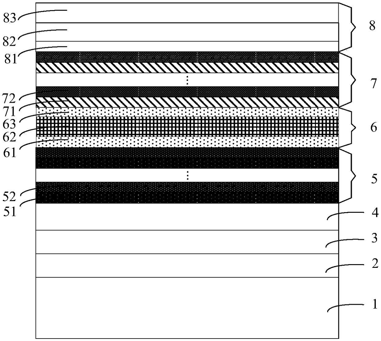
[0032] An embodiment of the present invention provides a light emitting diode epitaxial wafer, figure 1 It is a schematic structural diagram of a light-emitting diode epitaxial wafer provided by an embodiment of the present invention, as shown in figure 1 As shown, the light-emitting diode epitaxial wafer includes a substrate 1, a buffer layer 2, an undoped GaN layer 3, an N-type layer 4, a stress release layer 5, a multi-quantum well layer 7 and a P Type layer 8. The multi-quantum well layer 7 is a multi-period superlattice structure, and each superlattice structure includes an InGaN quantum well layer 71 and a GaN quantum barrier layer 72 grown on the InGaN quantum well layer 71 . The stress release layer 5 is a multi-period superlattice structure, and each superlattice structure includes a GaN layer 51 and an InGaN layer 52 grown on the GaN layer 51 .

[0033] The light-emitting diode epitaxial wafer also includes an electric field regulation layer 6 arranged between the ...

Embodiment 2

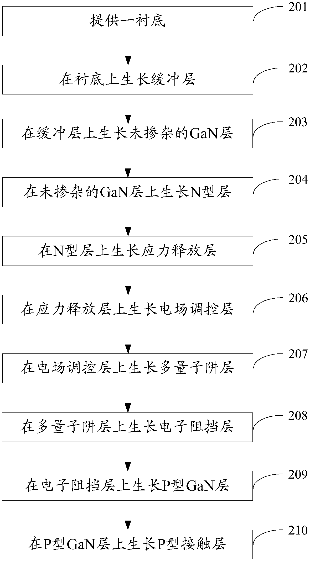
[0053] An embodiment of the present invention provides a method for manufacturing a light-emitting diode epitaxial wafer, which is used to manufacture the light-emitting diode epitaxial wafer provided in Embodiment 1, figure 2 It is a method flowchart of a method for manufacturing a light-emitting diode epitaxial wafer provided by an embodiment of the present invention, as shown in figure 2 As shown, the manufacturing method includes:

[0054] Step 201, providing a substrate.

[0055] In this embodiment, the substrate is sapphire.

[0056] Step 201 also includes:

[0057] The temperature of the reaction chamber is controlled at 1050° C., the pressure is 200-500 Torr, the sapphire substrate is annealed in a pure hydrogen atmosphere for 5-6 minutes, and then the sapphire substrate is nitrided.

[0058] In this embodiment, Veeco K465i or C4 MOCVD (Metal Organic Chemical Vapor Deposition, Metal Organic Compound Chemical Vapor Deposition) equipment can be used to realize the L...


PUM


Abstract

The invention discloses a light emitting diode epitaxial wafer and a manufacturing method thereof, belonging to the field of semiconductor technology. The LED epitaxial wafer comprises a substrate, abuffer layer, an undoped GaN layer, an N-type layer, a stress relief layer, an electric field regulating layer, a multiple quantum well layer and a P-type layer, wherein the electric field regulatinglayer is a sandwich structure of Mg doped GaN / AlN / GaN. The LED epitaxial wafer comprises a substrate, a buffer layer, an undoped GaN layer, an N-type layer, a stress relief layer, an electric field regulating layer and a P-type layer. Doped with Mg in the electric field control layer, holes can be generated to consume some electrons in advance, reduce the electron concentration, and prevent the electrons from overflowing into the P-type layer due to the high concentration after moving to the multiple quantum well layer. At the same time, it can also reduce the intensity of the built-in electric field of the multiple quantum well layer, reduce the blocking effect on the holes, and improve the hole injection efficiency. And the AlN layer in the electric field control layer can raise the electron barrier, reduce the electron migration rate, and reduce the electron overflow. Finally, more electrons and holes can recombine in the multi-quantum well layer, which improves the luminescence efficiency of LEDs.

Description

technical field [0001] The invention relates to the technical field of semiconductors, in particular to a light-emitting diode epitaxial wafer and a manufacturing method thereof. Background technique [0002] LED (Light Emitting Diode, Light Emitting Diode) is a semiconductor electronic component that can emit light. As an efficient, environmentally friendly and green new solid-state lighting source, it is being rapidly and widely used, such as traffic lights, car interior and exterior lights, urban landscape lighting, mobile phone backlights, etc. [0003] The epitaxial wafer is the main component of the LED. The existing GaN-based LED epitaxial wafer includes a substrate and a buffer layer stacked on the substrate in sequence, an undoped GaN layer, an N-type layer, a stress release layer, and multiple quantum wells. layer and P-type layer. Among them, the N-type layer is doped with Si to provide electrons; the P-type layer is doped with Mg to provide holes; when a curren...

Claims


Application Information

Patent Timeline
Patent Type & Authority Applications(China)
IPC IPC(8): H01L33/06H01L33/12H01L33/14H01L33/00
CPCH01L33/007H01L33/06H01L33/12H01L33/14
Inventor 唐成双李昱桦张燕飞刘春杨胡加辉
Owner HC SEMITEK ZHEJIANG CO LTD
Why Eureka
Try Eureka