Stacked spiral inductor

A technology of spiral inductance and inductance, applied in the direction of inductors, printed inductors, fixed inductors, etc., can solve the problems of low performance and large parasitic capacitance

Active Publication Date: 2019-01-15
CSMC TECH FAB2 CO LTD
View PDF5 Cites 3 Cited by
  • Summary
  • Abstract
  • Description
  • Claims
  • Application Information

AI Technical Summary

Problems solved by technology

[0003] Based on this, it is necessary to address the problems of large parasitic capacitance and low performance between metal layers, and provide a method that can improve the performance of spiral inductors on the same substrate area without changing the existing process technology. Stacked Spiral Inductor

Method used


Image

  • Stacked spiral inductor
  • Stacked spiral inductor
  • Stacked spiral inductor

Examples


Embodiment Construction

[0023] In order to make the object, technical solution and advantages of the present invention clearer, the present invention will be further described in detail below in conjunction with the accompanying drawings and embodiments. It should be understood that the specific embodiments described here are only used to explain the present invention, not to limit the present invention.

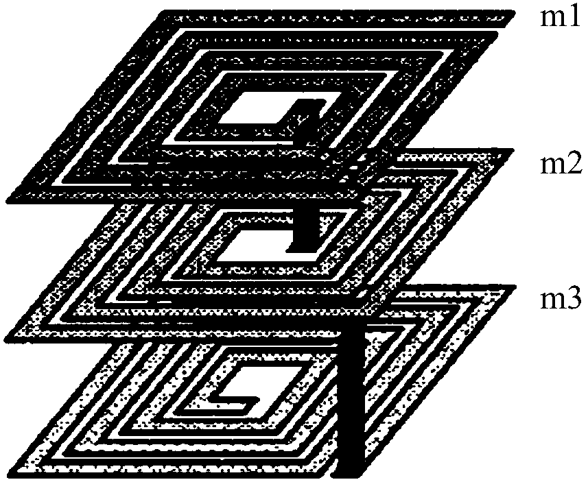
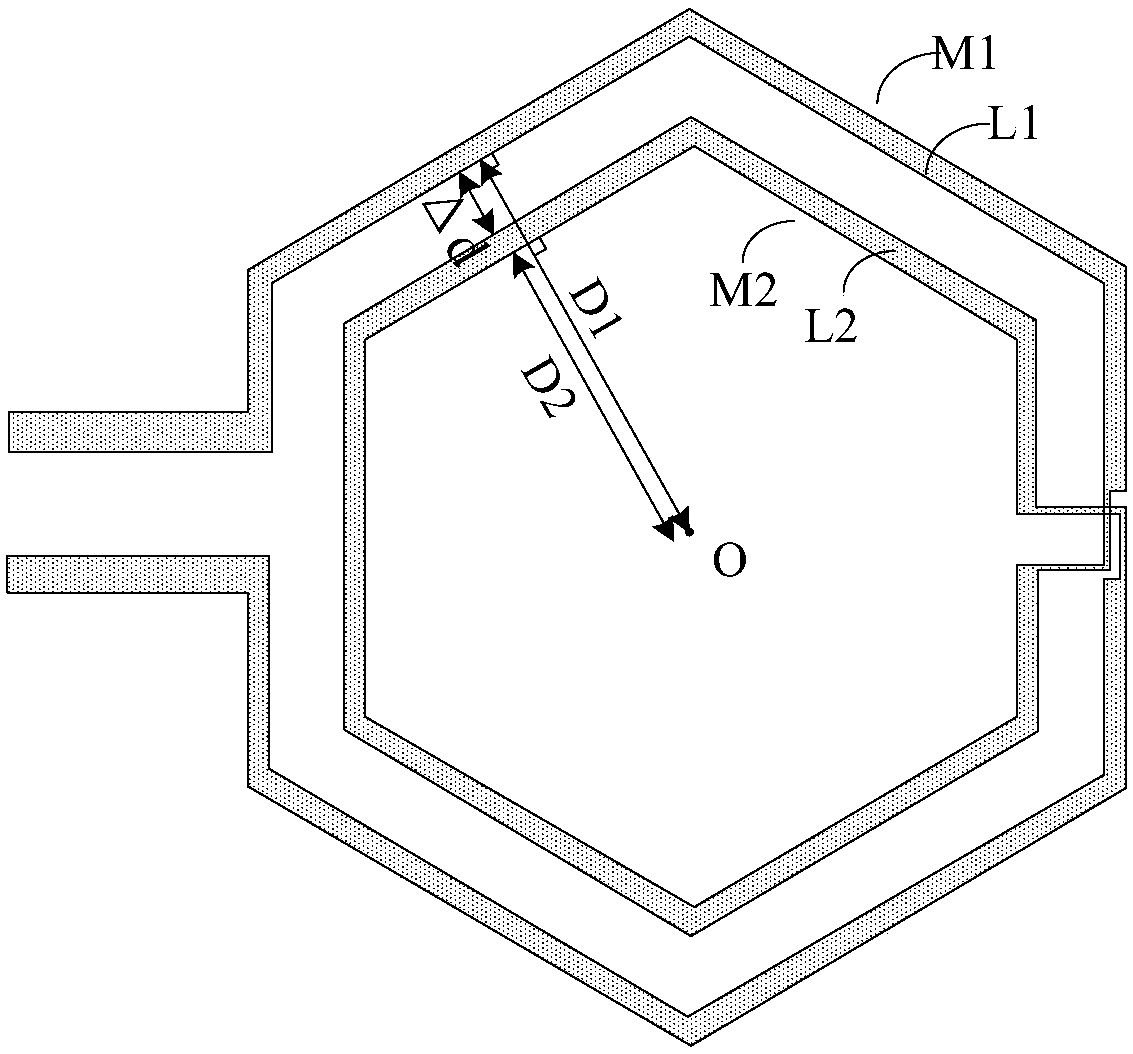
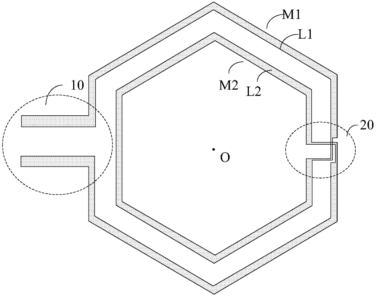
[0024] A stacked spiral inductor includes a substrate and a multi-layer stacked insulating layer and an inductive metal layer formed on the substrate through a semiconductor process.

[0025] Wherein, the substrate may be a silicon substrate, or may be gallium arsenide, germanium silicide or other semiconductor substrates. The insulating layer is formed by deposition or epitaxy on the substrate, and the insulating layer may be a silicon dioxide layer, or a silicon nitride layer or other insulating oxide layers. Etching the insulating layer to form a through hole, sputtering on the insulating layer...


PUM


Abstract

A stacked spiral inductor includes a substrate and a plurality of stac insulating layers and an inductive metal layer for on that substrate by a semiconductor process. The stacking spiral inductor includes a substrate and a plurality of layers of insulating layers and an inductive metal layer formed on the substrate by a semiconductor process. The inductive metal layer includes a conductive coil having a spiral shape and a via region for connecting two adjacent inductive metal layers, The conductive coils of each of the inductive metal layers have a common coil center, and the conductive coilsof the lower inductive metal layer are retracted toward the coil center with respect to the conductive coils of the upper inductive metal layer in two adjacent inductive metal layers. The parasitic capacitance between the layers of the spiral inductor is reduced without changing the conditions of the prior art and with the same substrate area, the self-resonant frequency is increased, and the performance of the spiral inductor is further improved.

Description

technical field [0001] The invention relates to the technical field of semiconductors, in particular to stacked spiral inductors. Background technique [0002] The traditional stacked spiral inductor is prepared by preparing a planar spiral inductor on each metal layer, and then connecting the spiral inductors of two adjacent layers through metal vias, such as figure 1 As shown, it becomes a stacked spiral inductor with three metal layers connected to each other. Wherein, the shapes and sizes of the planar spiral inductors in the first metal layer m1 , the second metal layer m2 , and the third metal layer m3 are all the same. In traditional stacked spiral inductors, the parasitic capacitance of the planar spiral inductor between the metal layers is large, and the parasitic coupling capacitance between the metal layer and the silicon substrate will also become large, which seriously affects the performance of the stacked spiral inductor. Contents of the invention [0003]...

Claims


Application Information

Patent Timeline
Patent Type & Authority Applications(China)
IPC IPC(8): H01L23/522
CPCH01L23/5227H01L23/12H01F17/0013H01F2017/0073H01F2017/008H01F2017/0086
Inventor 董聪颖
Owner CSMC TECH FAB2 CO LTD
Why Eureka
Try Eureka