
Method for cleanly transferring single layer graphene by using PMMA

A single-layer graphene and graphene technology, applied in the direction of single-layer graphene, graphene, chemical instruments and methods, etc., can solve the problems of unstable growth, easy curling, incomplete transfer graphene method, etc., and achieve roughness Low, reduce the force, show the effect of cleaning

Inactive Publication Date: 2019-01-18
HARBIN INST OF TECH
View PDF3 Cites 11 Cited by
  • Summary
  • Abstract
  • Description
  • Claims
  • Application Information

AI Technical Summary

Problems solved by technology

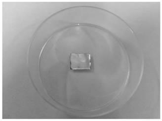
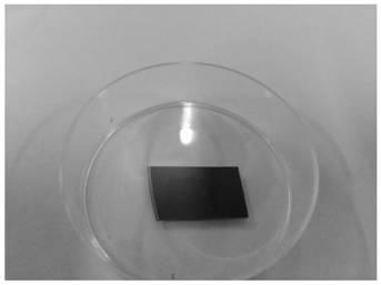
[0007] The present invention will solve the problem of unstable growth of existing graphene on specific substrates (such as silicon wafers with an oxide layer on the surface and substrates with some volatile or unstable substances on the surface) and the existence of transfer graphene methods. incomplete, curl-prone problem; instead, a method for clean transfer of single-layer graphene using PMMA is provided

Method used


Image

  • Method for cleanly transferring single layer graphene by using PMMA
  • Method for cleanly transferring single layer graphene by using PMMA
  • Method for cleanly transferring single layer graphene by using PMMA

Examples


Embodiment 1

[0040] Embodiment 1: utilize the method for PMMA to cleanly transfer single-layer graphene in the present embodiment to be accomplished through the following steps:

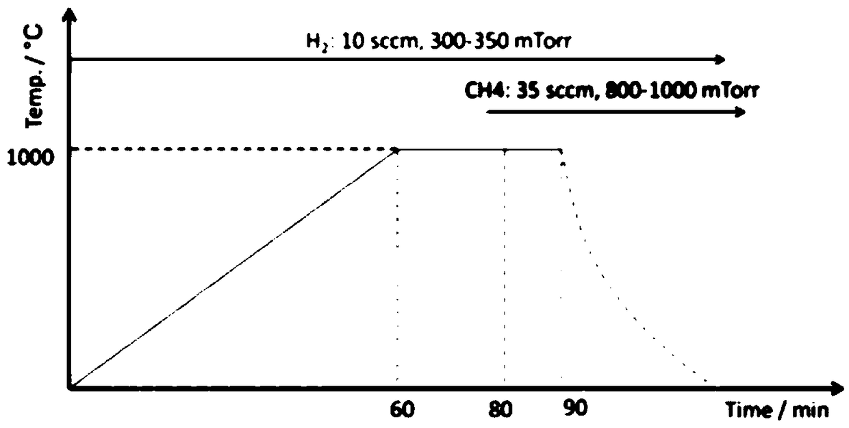
[0041] Step 1, using CVD to grow single-layer graphene on the copper foil substrate;

[0042] Step 2, stick the copper foil with single-layer graphene on the quartz plate with adhesive tape, then spin coat PMMA glue on the graphene surface on the copper foil substrate with 2500rpm, spin coat 100s to obtain the PMMA glue layer thickness is about 200nm, then Put it on a heating plate and heat at 160°C for 2 minutes to solidify the PMMA glue on the graphene surface, and then cut the edge to expose the graphene; the PMMA glue can be prepared in the following way: use anisole as a solvent and add PMMA powder to prepare into a solution with a concentration of 55mg / mL, and stirred evenly at 70°C until the color of the solution changed from milky white to transparent;

[0043] Step 3. Float the copper foil on the surfac...

Embodiment 2

[0053] Embodiment 2: the method utilizing PMMA to cleanly transfer single-layer graphene is accomplished through the following steps in the present embodiment:

[0054] Step 1, using CVD to grow single-layer graphene on the copper foil substrate;

[0055] Step 2, stick the copper foil with single-layer graphene on the quartz plate with adhesive tape, then spin coat PMMA glue on the graphene surface on the copper foil substrate with 3500rpm, spin coat 60s to obtain the PMMA glue layer thickness is about 100nm, then Put it on a heating plate and heat it at 200°C for 1 min to solidify the PMMA glue on the graphene surface, and then cut the edge to expose the graphene; the PMMA glue can be prepared in the following way: use anisole as a solvent and add PMMA powder to prepare into a solution with a concentration of 50mg / mL, and stir evenly at 75°C until the color of the solution changes from milky white to transparent;

[0056] Step 3. Float the copper foil on the surface of the f...


PUM

PropertyMeasurementUnit
elastic modulusaaaaaaaaaa

Abstract

The invention discloses a method for cleanly transferring single layer graphene by using PMMA, and relates to a method for transferring the single layer graphene, aiming to solve the problems of an existing graphene transferring method that existing graphene grows unstably on a specific substrate such as a silicon wafer and the transferring is incomplete and curling easily occurs. The method disclosed by the invention is as follows: first, single layer graphene is grown on a copper foil substrate; second, then the copper foil substrate is coated with a PMMA glue in a suspending way, and then placed on a heating plate, heated, solidified, and trimmed; third, the copper foil is floated on the liquid-level of corrosive liquid, and fished out until the copper foil becomes transparent; fourth,standing in water is performed; fifth, the operation of the fourth step is repeated; sixth, the target substrate is picked up, blow-dried with nitrogen, and baked in an oven until the surface turns purple; seventh, PMMA is added dropwise, and standing is performed; and eighth, soaking in acetone, heating and washing are performed to complete the transfer of the single layer graphene. The method disclosed by the invention has broad prospects in the fields of optoelectronic devices and the like.

Description

technical field [0001] The invention relates to a method for transferring single-layer graphene; in particular, it relates to a method for using PMMA to cleanly transfer single-layer graphene. Background technique [0002] Graphene is a new carbonaceous material that is tightly packed into a two-dimensional honeycomb lattice structure by a single layer of carbon atoms. Its energy band structure has a linear dispersion relationship, and the top of the valence band and the bottom of the conduction band are at the Dirac point. Overlapping has incomparable advantages over traditional materials in electronic devices. [0003] First of all, graphene has a perfect hybrid structure, and its large conjugated system makes its electron transport ability very strong; studies have shown that the electron conduction rate in graphene is as high as 8*105m*s -1 , electrons can travel submicron distances without scattering. Secondly, the electrons and holes in graphene are separated from ea...

Claims


Application Information

Patent Timeline
Patent Type & Authority Applications(China)
IPC IPC(8): C01B32/194C01B32/186
CPCC01B2204/02C01B32/186C01B32/194
Inventor 张墅野何鹏胡平安林铁松张彦鑫
Owner HARBIN INST OF TECH
Learn More