A preparation method of a low-cost P-type all-back-electrode crystalline silicon solar cell

A crystalline silicon solar cell and full-back electrode technology, applied in the field of solar cells, can solve the problems of relatively high minority carrier life requirements, different doping types, complex process flow, etc. effect of steps

Pending Publication Date: 2019-01-18
RISEN ENERGY (CHANGZHOU) CO LTD
View PDF0 Cites 8 Cited by
  • Summary
  • Abstract
  • Description
  • Claims
  • Application Information

AI Technical Summary

Problems solved by technology

Since the electrodes of IBC batteries are all on the back side, the photogenerated carriers need to move to the back side to be collected. Therefore, the requirements for the minority carrier life of the substrate are relatively high. Companies or institutions that mass produce or develop IBC batteries often choose N-type cells with high minority carrier life. Crystalline silicon wafers are used as substrates, but the price of N-type silicon wafers is higher than that of P-type silicon wafers
Another disadvantage of N-type IBC cells is that the back field and emitter junction regions on the back need to be doped, and the doping types are different, which leads to a complicated process and high production costs.

Method used


Image

  • A preparation method of a low-cost P-type all-back-electrode crystalline silicon solar cell

Examples


Embodiment Construction

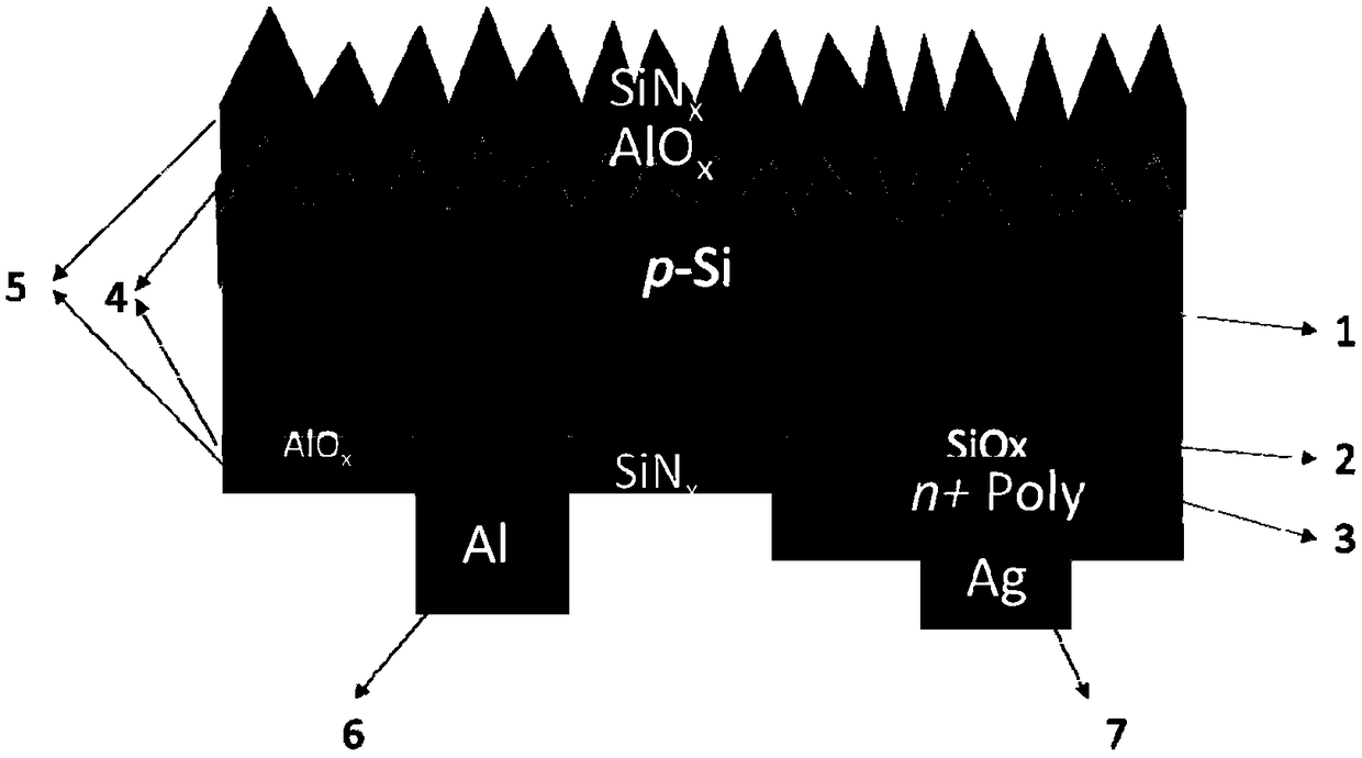
[0032] The present invention is described in further detail now in conjunction with accompanying drawing. These drawings are all simplified schematic diagrams, which only illustrate the basic structure of the present invention in a schematic manner, so they only show the configurations related to the present invention.

[0033] Such as figure 1 As shown, a low-cost P-type all-back electrode crystalline silicon solar cell, the specific structure is as follows:

[0034] (1) The battery uses a P-type monocrystalline silicon wafer as the substrate 1, such as figure 1 As shown in the middle area 1, the resistivity of the silicon wafer is 1-5ohm·cm, the front of the silicon wafer is pyramid-shaped suede, and the back is a polished plane;

[0035] (2) The emitter junction area on the back of the battery has a tunnel oxide layer 2, such as figure 1 As shown in the middle area 2, the thickness of the oxide layer is 1-2nm, and a tunneling contact can be formed;

[0036] (3) A heavil...


PUM


Abstract

The invention relates to the technical field of solar cells, in particular to a preparation method of a low-cost P-type all-back-electrode crystalline silicon solar cell. The method includes such steps as polishing or velveting P-type single crystal silicon wafer as silicon substrate, growing tunneling silicon oxide film and intrinsic polycrystalline silicon film on both sides of battery, depositing SiNx film on back side of battery by phosphorus diffusion, and ablating silicon nitride on back side of battery by laser; Flocking treatment, removing the mask silicon nitride and phosphor-siliconglass in the back junction region, depositing aluminum oxide film on both sides, depositing silicon nitride film on the front and back sides of the battery respectively, laser ablating part of aluminum oxide / silicon nitride film in the back back field region to form a local aluminum back field, and adopting a back silver + aluminum paste structure in the back field region; The preparation method of the full-back electrode solar cell of the invention has the advantages of high efficiency, less silver paste consumption, no boron diffusion and other expensive processes, and low battery productioncost.

Description

technical field [0001] The invention relates to the technical field of solar cells, in particular to a method for preparing low-cost P-type crystal silicon solar cells with full back electrodes. Background technique [0002] Interdigitated Back Contact solar cells (IBC) have much higher efficiency than conventional solar cells because of the absence of grid lines on the front. As early as 2012, the efficiency of IBC batteries produced by Sunpower in the United States reached 24%. In recent years, its efficiency has increased to more than 25%. Since the electrodes of IBC batteries are all on the back side, the photogenerated carriers need to move to the back side to be collected. Therefore, the requirements for the minority carrier life of the substrate are relatively high. Companies or institutions that mass produce or develop IBC batteries often choose N-type cells with high minority carrier life. Crystalline silicon wafers are used as substrates, but the price of N-type s...

Claims


Application Information

Patent Timeline
IPC IPC(8): H01L31/18H01L31/0224
CPCH01L31/022441H01L31/1804Y02E10/547Y02P70/50
Inventor 袁声召崔艳峰万义茂黄强林海峰
Owner RISEN ENERGY (CHANGZHOU) CO LTD
Why Eureka
Try Eureka