Inclined silicon groove etching process
A dipped silicon technology, which is applied in the manufacture of electrical components, semiconductor/solid-state devices, circuits, etc., can solve the problems of inability to meet the isolation requirements of bipolar integrated circuits, affect the performance and reliability of three-dimensional integrated devices, and increase leakage, and achieve Optimizing the morphology of silicon grooves, eliminating voids, and improving the breakdown voltage
- Summary
- Abstract
- Description
- Claims
- Application Information
AI Technical Summary
Problems solved by technology
Method used
Image


Examples
Embodiment 1
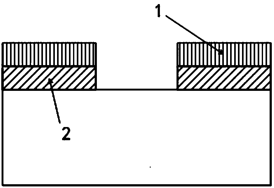
[0044] Step 1: grow a 13 μm epitaxial layer on the surface of p-100 type SOI substrate, and then grow 1 μm SiO in the furnace tube 2 , using SiO 2 As a hard mask layer 2 for silicon trench etching, the SiO 2 The surface is coated with photoresist to form a photoresist layer 1, exposed and developed to expose the SiO that needs to be etched 2 Window, the window pattern is a groove, the groove width is 0.8μm;
[0045]Step 2: Use CENTURA5200 silicon dioxide plasma dry etching machine; wherein, the chamber pressure is 200mT, the electrode power is 600W, and the process gas includes CHF with a flow rate of 30sccm 3 , CF with a flow rate of 30sccm 4 and Ar at a flow rate of 150 sccm, etch all the way to the wafer surface.
[0046] After 240s, the etching of the hard mask is completed.
[0047] Step 3: Use CENTURA5202 dry etching machine for silicon etching, that is, deep silicon groove etching. Set the silicon groove etching bias power to 50W, the frequency to 120Hz, the bias ...
Embodiment 2
[0052] Step 1: grow a 13 μm epitaxial layer on the surface of p-100 type SOI substrate, and then grow 1 μm SiO in the furnace tube 2 , using SiO 2 As a hard mask layer 2 for silicon trench etching, the SiO 2 The surface is coated with photoresist to form a photoresist layer 1, exposed and developed to expose the SiO that needs to be etched 2 Window, the window pattern is a groove, the groove width is 1.0μm;
[0053] Step 2: Use CENTURA5200 silicon dioxide plasma dry etching machine; wherein, the chamber pressure is 200mT, the electrode power is 600W, and the process gas includes CHF with a flow rate of 30sccm 3 , CF with a flow rate of 30sccm 4 and Ar at a flow rate of 150 sccm, etch all the way to the wafer surface.
[0054] After 240s, the etching of the hard mask is completed.
[0055] Step 3: Use CENTURA5202 dry etching machine for silicon etching, that is, deep silicon groove etching. Set the silicon groove etching bias power to 55W, the bias power frequency to 110H...
Embodiment 3
[0060] Step 1: grow a 13 μm epitaxial layer on the surface of p-100 type SOI substrate, and then grow 1 μm SiO in the furnace tube 2 , using SiO 2 As a hard mask layer 2 for silicon trench etching, the SiO 2 The surface is coated with photoresist to form a photoresist layer 1, exposed and developed to expose the SiO that needs to be etched 2 Window, the window pattern is a groove, the groove width is 1.4μm;
[0061] Step 2: Use CENTURA5200 silicon dioxide plasma dry etching machine; wherein, the chamber pressure is 200mT, the electrode power is 600W, and the process gas includes CHF with a flow rate of 30sccm 3 , CF with a flow rate of 30sccm 4 and Ar at a flow rate of 150 sccm, etch all the way to the wafer surface.
[0062] After 240s, the etching of the hard mask is completed.
[0063] Step 3: Use CENTURA5202 dry etching machine for silicon etching, that is, deep silicon groove etching. Set the silicon groove etching bias power to 52W, the bias power frequency to 130H...
PUM
 Abstract
Description
Claims
Application Information
 - R&D
- Intellectual Property
- Life Sciences
- Materials
- Tech Scout
- Unparalleled Data Quality
- Higher Quality Content
- 60% Fewer Hallucinations
Browse by: Latest US Patents, China's latest patents, Technical Efficacy Thesaurus, Application Domain, Technology Topic, Popular Technical Reports.
© 2025 PatSnap. All rights reserved.Legal|Privacy policy|Modern Slavery Act Transparency Statement|Sitemap|About US| Contact US: help@patsnap.com