Organic electroluminescence device and display device

A technology for electroluminescent devices and organic light-emitting layers, applied in organic light-emitting devices, organic light-emitting device parameters, organic semiconductor devices, etc., can solve the problems of poor color purity, short device life, large efficiency roll-off, etc., and reduce efficiency. Roll-off, balanced transmission, the effect of promoting energy transfer

Active Publication Date: 2019-02-15
KUNSHAN GO VISIONOX OPTO ELECTRONICS CO LTD +1
View PDF4 Cites 15 Cited by
  • Summary
  • Abstract
  • Description
  • Claims
  • Application Information

AI Technical Summary

Problems solved by technology

[0004] The invention provides an organic electroluminescence device and a display device. The organic light-emitting layer of the device uses an exciplex as a host material to sensitize a resonant TADF...

Method used


Image

  • Organic electroluminescence device and display device
  • Organic electroluminescence device and display device
  • Organic electroluminescence device and display device

Examples


preparation example Construction

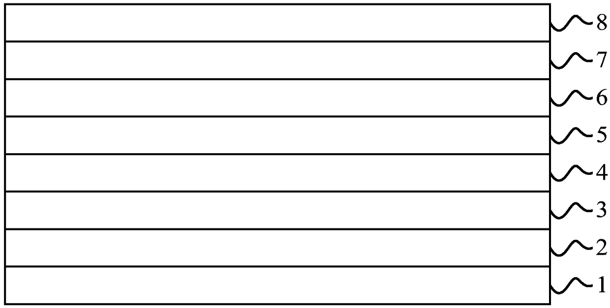
[0089] The present invention also provides a preparation method of the organic electroluminescent device, to figure 1 As an example, it includes sequentially depositing an anode 2 , a hole transport region 3 , an organic light-emitting layer 4 , an electron transport region 5 , and a cathode 6 on a substrate 1 , and then packaging. Wherein, when preparing the organic light emitting layer 4, the organic light emitting layer 4 is formed by co-evaporating the electron donor type material source, the electron acceptor type material source and the resonance type TADF material source.

[0090] Specifically, the preparation method of the organic electroluminescent device of the present invention comprises the following steps:

[0091] 1. Ultrasonically treat the glass plate coated with the anode material in a commercial cleaning agent, rinse in deionized water, ultrasonically degrease in acetone: ethanol mixed solvent, bake in a clean environment until the water is completely removed...

Embodiment 1

[0100] The device structure of this embodiment is as follows:

[0101] ITO / HI-2(10nm) / HT-27(40nm) / (D-1:A-6=1:9):20wt%M-20(30nm) / ET-53(30nm) / LiF(0.5nm ) / Al(150nm)

[0102] Wherein, the anode is ITO; the material of the hole injection layer is HI-2, and the general total thickness is 5-30nm, which is 10nm in this embodiment; the material of the hole transport layer is HT-27, and the total thickness is generally 5-50nm, This embodiment is 40nm; the host material of the organic light-emitting layer is an exciplex, wherein the mass ratio of D-1 and A-6 is 1:9, the dye is a resonance type TADF material M-20 and the doping concentration is 20wt% , the thickness of the organic light-emitting layer is generally 1-60nm, and the present embodiment is 30nm; the material of the electron transport layer is ET-53, and the thickness is generally 5-30nm, and the present embodiment is 30nm; the electron injection layer and the cathode material are selected from LiF ( 0.5nm) and metallic alumi...

Embodiment 2

[0105] The device structure of this embodiment is as follows:

[0106] ITO / HI-2(10nm) / HT-27(40nm) / (D-1:A-6=4:6):20wt%M-20(30nm) / ET-53(30nm) / LiF(0.5nm ) / Al(150nm)


PUM

PropertyMeasurementUnit
Thicknessaaaaaaaaaa
Thicknessaaaaaaaaaa

Abstract

The invention provides an organic electroluminescence device and a display device. The organic electroluminescence device comprises an organic luminescent layer, wherein the organic luminescent layercomprises a main body material and a resonant thermal activation delayed fluorescence material; the main body material is an exciplex; the singlet state energy level of the exciplex is greater than that of the resonant thermal activation delayed fluorescence material, and the triplet state energy level of the exciplex is greater than that of the resonant thermal activation delayed fluorescence material. The organic electroluminescence device can overcome the defects of short device lifetime and wide spectrum caused by the fact that a traditional TADF material is used for luminescence at the present stage.

Description

technical field [0001] The invention relates to an organic electroluminescence device and a display device, belonging to the technical field of organic electroluminescence. Background technique [0002] Organic Light Emitting Diode (OLED) is a device that is driven by current to achieve the purpose of emitting light. Its main characteristics come from the organic light-emitting layer. When an appropriate voltage is applied, electrons and holes Excitons are combined in the organic light-emitting layer to emit light of different wavelengths according to the characteristics of the organic light-emitting layer. At present, the light-emitting layer is composed of host materials and doped dyes, and the dyes are mostly selected from traditional fluorescent materials and traditional phosphorescent materials. Specifically, traditional fluorescent materials have the disadvantage of being unable to utilize triplet excitons. Although traditional phosphorescent materials can achieve 100...

Claims


Application Information

Patent Timeline
IPC IPC(8): H01L51/50H01L51/54
CPCH10K85/00H10K50/00H10K50/11H10K2101/10H10K85/631H10K85/654H10K85/322H10K85/40H10K85/6572H10K2101/90H10K2101/00H10K2101/20H10K85/633
Inventor 段炼蔡明瀚宋晓增李国孟
Owner KUNSHAN GO VISIONOX OPTO ELECTRONICS CO LTD
Why Eureka
Try Eureka