High-efficiency grating coupler based on intermediate-refractive-index waveguide material and preparation method therefor

A grating coupler and refractive index technology, applied in the direction of optical waveguide light guide, light guide, optics, etc., can solve the problems of complex processing technology and low coupling diffraction efficiency, and achieve the effect of simple process steps, high diffraction coupling efficiency and mature technology

Inactive Publication Date: 2019-02-19
SUN YAT SEN UNIV
View PDF9 Cites 18 Cited by
  • Summary
  • Abstract
  • Description
  • Claims
  • Application Information

AI Technical Summary

Problems solved by technology

[0007] The above-mentioned main reason for limiting the performance of grating couplers such as lithium niobate and silicon nitride is that lithium niobate and silicon nitride are medium refractive index materials (n~1.9-2.2), and rely solely on etching gratings in waveguide mat

Method used


Image

  • High-efficiency grating coupler based on intermediate-refractive-index waveguide material and preparation method therefor
  • High-efficiency grating coupler based on intermediate-refractive-index waveguide material and preparation method therefor
  • High-efficiency grating coupler based on intermediate-refractive-index waveguide material and preparation method therefor

Examples


Example Embodiment

[0035] Example 1

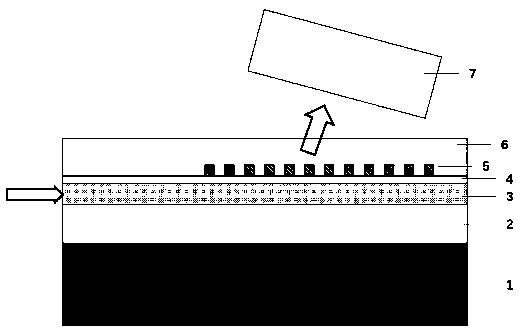
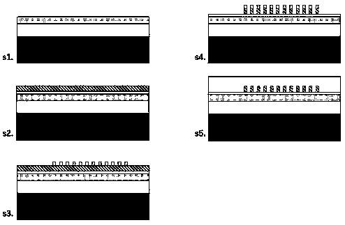
[0036] A high-efficiency grating coupler based on medium refractive index waveguide material, please refer to figure 1 , Including a substrate 1, a lower cladding layer 2, a medium refractive index material layer 3, an insulating layer 4, an amorphous silicon grating 5 and an upper cladding layer 6; wherein the structure of the grating coupler is the substrate 1 from bottom to top , Lower cladding layer 2, medium refractive index material layer 3, insulating layer 4, amorphous silicon grating 5, upper cladding layer 6. The light is transmitted in the medium refractive index material 3 in the waveguide mode. When the light is transmitted to the grating area and is diffracted by the amorphous silicon grating 5, the light wave meeting the Bragg condition is emitted at a specific angle and collected by the single-mode fiber 7. On the contrary, the light injected from the single-mode optical fiber 7 is coupled into the medium refractive index material waveguide 3 th...


PUM

PropertyMeasurementUnit
Thicknessaaaaaaaaaa
Thicknessaaaaaaaaaa
Thicknessaaaaaaaaaa

Abstract

The invention discloses a high-efficiency grating coupler based on an intermediate-refractive-index waveguide material. The specific structure is a substrate, a lower cladding layer, an intermediate-refractive-index material layer, an insulating layer, an amorphous silicon grating, and an upper cladding layer from bottom to top. The invention also discloses a preparation method of the high-efficiency grating coupler based on the intermediate-refractive-index waveguide material. The method comprises the following steps of: first preparing a waveguide lower cladding layer and the intermediate-refractive-index material layer on the substrate; implementing a waveguide device in the intermediate-refractive-index material layer; growing an insulating layer and amorphous silicon on a surface of asample; transferring a grating structure to an electron beam glue or a photoresist layer by an electron beam or an ultraviolet exposure, and forming a grating pattern after development; and then transferring the grating structure to the amorphous silicon grating by an etching process; and finally, removing the electron beam glue or the photoresist layer, and growing the upper cladding layer. Theinvention has the advantages of simpler process steps, lower cost and higher tolerance of errors.

Description

technical field [0001] The invention relates to the field of photonic devices and preparation methods thereof, more specifically, to a high-efficiency grating coupler based on a medium refractive index waveguide material and a preparation method thereof. Background technique [0002] Medium refractive index materials, such as lithium niobate and silicon nitride, have the characteristics of high transmittance and low loss from the visible to the mid-infrared range, and are ideal light transmission materials in integrated optoelectronic devices. [0003] For the crystal material lithium niobate thin film, the traditional coupling method between the optical fiber and the lithium niobate waveguide is to inject light into the waveguide from the end face after the wafer is cleaved. Submicron waveguide modes such as lithium niobate, silicon nitride, etc., generally do not match the mode of the fiber with microlenses, resulting in low coupling efficiency. The unilateral coupling ef...

Claims


Application Information

Patent Timeline
IPC IPC(8): G02B6/12G02B6/132G02B6/136G02B6/138
CPCG02B6/12002G02B6/132G02B6/136G02B6/138
Inventor 陈晖简健许鹏飞余思远
Owner SUN YAT SEN UNIV
Why Eureka
Try Eureka