
Organic Electroluminescent Devices

An electroluminescence device and a luminescence technology, applied in the direction of organic semiconductor devices, electric solid devices, electrical components, etc., can solve problems such as poor luminous efficiency, achieve enhanced hole injection efficiency, reduce hole injection barriers, The effect of improving performance

Active Publication Date: 2020-06-02
KUNSHAN GO VISIONOX OPTO ELECTRONICS CO LTD +1
View PDF2 Cites 0 Cited by
  • Summary
  • Abstract
  • Description
  • Claims
  • Application Information

AI Technical Summary

Problems solved by technology

[0006] The technical problem to be solved by the present invention is to overcome the defects of poor luminous efficiency of organic electroluminescent devices in the prior art

Method used


Image

  • Organic Electroluminescent Devices
  • Organic Electroluminescent Devices
  • Organic Electroluminescent Devices

Examples


Embodiment 1

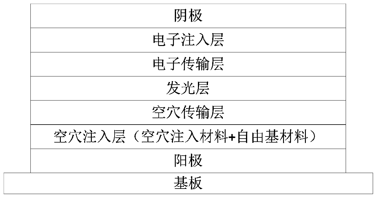
[0046] The embodiment of the present invention provides an organic electroluminescent device, such as figure 1 As shown, the organic electroluminescent device includes a first electrode, a hole injection layer, a hole transport layer, a light emitting layer, an electron transport layer, an electron injection layer, and a second electrode stacked on a substrate.

[0047] Wherein, the hole injection layer includes at least one hole injection material and at least one free radical molecular material doped in the hole injection material. Among them, the free radical molecule is an open-shell molecule with unpaired electrons and electron vacancies on its single-occupied molecular orbital (Singly Occupied Molecular Orbital, referred to as SOMO). In this embodiment, the hole injection material of the organic electroluminescent device can be selected from LUMO energy level materials, and the LUMO orbital energy level is less than or equal to -5.5 eV. For example, it can be HAT-CN or MoO ...

Embodiment 2

[0068] This embodiment provides an organic electroluminescent device. The specific structure is the same as that of Embodiment 1. The difference is that the radical molecular material is of formula (2), the doping concentration of the radical molecular material is 20wt%, and the hole injection layer The thickness is 20nm.

Embodiment 3

[0070] This embodiment provides an organic electroluminescent device. The specific structure is the same as that of Embodiment 1. The difference is that the radical molecular material is of formula (3), the doping concentration of the radical molecular material is 15wt%, and the hole injection layer The thickness is 50nm.


PUM

PropertyMeasurementUnit
thicknessaaaaaaaaaa

Abstract

The invention relates to the technical field of display and provides an organic electroluminescent device. The organic electroluminescence device comprises a hole injection layer comprising at least one hole injection material and at least one radical molecular material doped in the hole injection material. By doping at least one free radical molecular material in the hole injection layer, due to the deep energy level characteristics of the hole injection material and its strong ability to absorb electrons, the single electron on the free radical molecular material transitions to the hole injection material On the LUMO of the hole injection layer, charge transfer occurs in the hole injection material to form free holes, thereby achieving the purpose of improving the conductivity of the hole injection layer, effectively reducing the hole injection barrier, enhancing the hole injection efficiency, and improving performance of organic electroluminescent devices.

Description

Technical field [0001] The invention relates to the field of display technology, in particular to an organic electroluminescence device. Background technique [0002] Organic Light-Emitting Device (Organic Light-Emitting Device, OLED for short) is an active light-emitting device with the advantages of low power consumption, wide color gamut, and thinner volume. It is expected to become the next generation of mainstream lighting and flat panel display technology. [0003] A commonly used OLED includes a first electrode, an organic light-emitting layer, and a second electrode stacked on a substrate. When the OLED is working, holes are injected into the device through the first electrode and electrons are injected into the device through the second electrode. The carriers in the highest occupied molecular orbital (HOMO) and the lowest unoccupied molecular orbital (LUMO) of the luminescent material combine to form excitons, which release their energy in the form of light. [0004] In t...

Claims


Application Information

Patent Timeline
Patent Type & Authority Patents(China)
IPC IPC(8): H01L51/50H01L51/54H01L51/56H10K99/00
CPCH10K85/00H10K50/11H10K2101/40H10K50/17H10K71/30H10K85/6572H10K85/631H10K85/60H10K85/636H10K2101/30H10K2102/351
Inventor 段炼宾正杨田景文
Owner KUNSHAN GO VISIONOX OPTO ELECTRONICS CO LTD
Learn More