
Phase inverter for tunneling transistor based on graphite, and preparation method thereof

A technology of tunneling transistors and inverters, which is used in transistors, semiconductor/solid-state device manufacturing, semiconductor devices, etc., can solve the problems of low saturation motion speed and difficult to meet the requirements of response speed of digital logic circuits, so as to improve the overall Gain, protect quality, improve the effect of regulating ability

Active Publication Date: 2019-03-12
SOUTHEAST UNIV
View PDF11 Cites 0 Cited by
  • Summary
  • Abstract
  • Description
  • Claims
  • Application Information

AI Technical Summary

Problems solved by technology

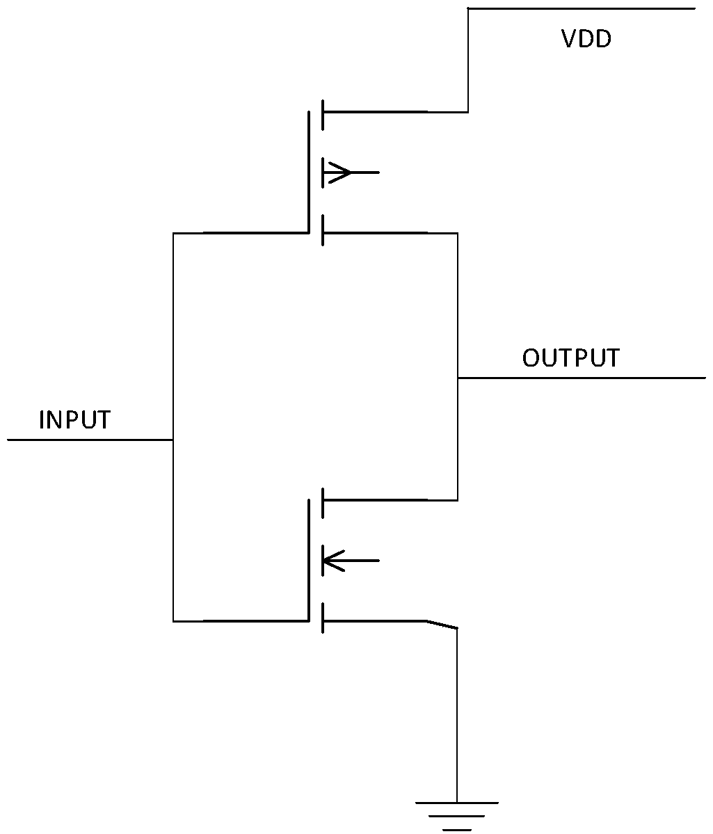
The existing CMOS inverter circuit consists of two enhanced MOS field effect transistors, such as figure 1 As shown, because the saturation movement speed of electrons in silicon is not high, it is difficult to meet the requirements of digital logic circuits for response speed in high-frequency operating mode

Method used


Image

  • Phase inverter for tunneling transistor based on graphite, and preparation method thereof
  • Phase inverter for tunneling transistor based on graphite, and preparation method thereof
  • Phase inverter for tunneling transistor based on graphite, and preparation method thereof

Examples


Embodiment Construction

[0030] Embodiments of the present invention are described in detail below, examples of which are shown in the drawings, wherein the same or similar reference numerals denote the same or similar elements or elements having the same or similar functions throughout. The embodiments described below by referring to the figures are exemplary only for explaining the present invention and should not be construed as limiting the present invention.

[0031] Those skilled in the art will understand that unless otherwise stated, the singular forms "a", "an", "said" and "the" used herein may also include plural forms. It should be further understood that the word "comprising" used in the description of the present invention refers to the presence of said features, integers, steps, operations, elements and / or components, but does not exclude the presence or addition of one or more other features, Integers, steps, operations, elements, components, and / or groups thereof. It will be understoo...


PUM

PropertyMeasurementUnit
electron work functionaaaaaaaaaa
thicknessaaaaaaaaaa
electron work functionaaaaaaaaaa

Abstract

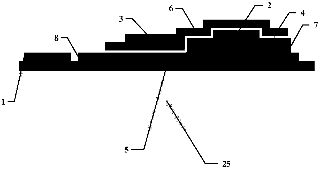
The invention discloses a phase inverter for a tunneling transistor based on graphite, and a preparation method thereof. The graphene tunneling transistor comprises a source electrode, a grid electrode, a drain electrode, a graphene film, a semiconductor or metal substrate, a tunneling layer, a drain electrode insulating layer, a grid electrode insulating layer, a graphene passivation layer and adirect current bias voltage source, wherein the source electrode and a silicon substrate are connected, the drain electrode and the graphene film are connected, one tunneling layer is arranged betweenthe graphene and the substrate, and the grid electrode is arranged on the top of an electron tunneling part. If the work function of the semiconductor or metal substrate is small, the drain electrodeselects metal with a large work function, and the device is of an n type; and otherwise, the drain electrode adopts the metal with the large work function, and the device is of a p type. The p-type pipe drain electrode is connected with a high level, an n-type pipe source electrode is connected with a low level, the common grid electrode of two pipes serves as the input end of a circuit, and a p-type pipe source electrode and an n-type pipe drain electrode are connected to serve as the output end of the circuit. By use of the novel graphene tunneling transistor structure, a digital logic phase inverter with a high response rate and low static power consumption is realized.

Description

technical field [0001] The invention relates to an inverter and a preparation method thereof, in particular to a graphite-based tunneling transistor inverter and a preparation method thereof, and belongs to the technical field of electronic device preparation. Background technique [0002] An inverter is an electronic device that can reverse the phase of an input signal, and is widely used in analog circuits, such as audio amplifier circuits, clock oscillators, etc. The existing CMOS inverter circuit consists of two enhanced MOS field effect transistors, such as figure 1 As shown, because the saturation movement speed of electrons in silicon is not high, it is difficult to meet the requirements of digital logic circuits for response speed in high-frequency operating mode. Contents of the invention [0003] In view of the above problems, the present invention provides a graphite-based tunneling transistor inverter with fast response and high gain and a preparation method t...

Claims


Application Information

Patent Timeline
Patent Type & Authority Applications(China)
IPC IPC(8): H01L29/739H01L29/16H01L29/06H01L27/082H01L21/8222H01L21/331
CPCH01L21/8222H01L27/082H01L29/0653H01L29/1606H01L29/66356H01L29/7391
Inventor 王琦龙杨文鑫徐季翟雨生张晓兵
Owner SOUTHEAST UNIV
Learn More