Bonding process for target material for liquid crystal display, semiconductor and electronics

A liquid crystal display and semiconductor technology, applied in metal material coating process, ion implantation plating, coating and other directions, can solve the problems of inability to create a working environment for workers and high working environment temperature, reduce energy consumption and reduce oxidation degree, the effect of reducing the ambient temperature

Inactive Publication Date: 2019-03-29
爱发科电子材料(苏州)有限公司
View PDF6 Cites 1 Cited by
  • Summary
  • Abstract
  • Description
  • Claims
  • Application Information

AI Technical Summary

Problems solved by technology

At present, when bonding high-purity targets for liquid crystal displays, semiconductors, and electronics and copper backplanes in the market, the bonding process of targets for liquid crystal displays, semiconductors, and electronics currently used cannot avoid the following two conditions: (1 ) The working environment temperature of the targe...

Method used


Image

  • Bonding process for target material for liquid crystal display, semiconductor and electronics
  • Bonding process for target material for liquid crystal display, semiconductor and electronics
  • Bonding process for target material for liquid crystal display, semiconductor and electronics

Examples


Embodiment 1

[0023] A bonding process of targets for liquid crystal displays, semiconductors, and electronics in this embodiment uses pure copper as the target and back plate. The purity of pure copper reaches 99.99%. The target size is 1350mm*250mm, and Board size: 1400mm*300mm. The bonding process includes the following steps:

[0024] Step 1, preparation of bonding material pure metal indium wire

[0025] Use sandpaper to polish the surface of the bonding material indium wire for 3 minutes, and there is no oxidation, rust and other impurities on the surface. The indium wire has a purity of 99.99%, a diameter of φ10.6mm, and is put into the melting machine straightly.

[0026] Step two, grinding operation

[0027] Grind the bonding surface required for the target and the back plate. For the first grinding, use 320# sandpaper to grind the target and the back plate for 3 to 5 minutes, and then use 150# sandpaper to grind the bonding surface of the target and the back plate for 3 to 5 mi...

Embodiment 2

[0042] The difference from the first embodiment is that the following parameters of the bonding process of a liquid crystal display, semiconductor, and electronic targets in this embodiment are different.

[0043] In Step 4, the injection rate is 10 m / min, and the injection temperature is 180°C.

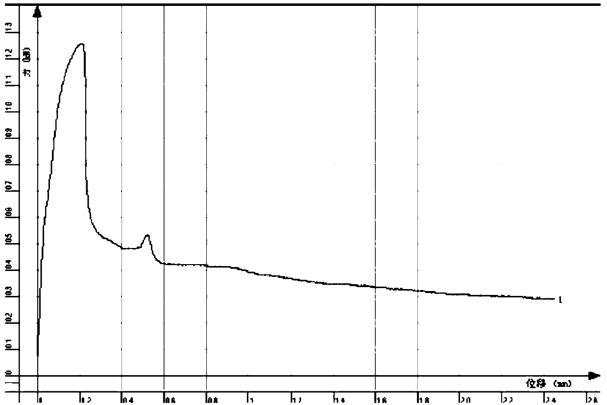
[0044] In step five, the pressure applied during cooling is 8KPa, and the cooling time is 20min. After the final test and analysis, such as image 3 , 4 As shown, the tensile strength of the adhesive layer reaches 1.01 MPa, and the good rate of the adhesive layer reaches 96.8%.

Embodiment 3

[0046]The difference from Example 1 is that the following parameters of the bonding process of a target for liquid crystal display, semiconductor, and electronics in this example are different

[0047] In Step 4, the injection rate is 30 m / min, and the injection temperature is 170°C.

[0048] In step five, the pressure applied during cooling is 7KPa, and the cooling time is 30min. After the final test and analysis, such as Figure 5 , 6 As shown, the tensile strength of the adhesive layer reaches 0.99MPa, and the good rate of the adhesive layer reaches 95.5%.


PUM

PropertyMeasurementUnit
Roughnessaaaaaaaaaa
Tensile strengthaaaaaaaaaa

Abstract

The invention discloses a bonding process for a target material for liquid crystal display, a semiconductor and electronics. The bonding process comprises the following sequentially performed steps that a bonding material preparation step is performed, wherein a pure metal indium wire is prepared; a plasma spraying step is performed, wherein the prepared pure metal indium wire is placed into a plasma spraying device to be heated to be in a molten state, and the molten-state pure metal indium is correspondingly sprayed on the corresponding surfaces of the target material and a back plate through the plasma spraying device; and a bonding step is performed, wherein the target material and the back plate which are subjected to surface spraying are bonded, and a preset pressure is applied to the upper surface of the bonded finished product for cooling. According to the bonding process, the oxidation of the bonding material can be reduced.

Description

technical field [0001] The invention relates to the field of target material production, in particular to a bonding process for liquid crystal display, semiconductor and electronic target materials. Background technique [0002] Liquid crystal is a special substance between solid and liquid. When an electric field is applied, its molecular arrangement will be changed. At this time, if it is equipped with a polarizer, it can prevent light from passing through. [0003] As the most important original of liquid crystal display, the production of thin film light-emitting diode (TFT) requires the target of liquid crystal display, semiconductor and electronic coating materials to be bonded by high-purity target and copper backplane. The acceptance rate is greater than or equal to 95%. At present, when bonding high-purity targets for liquid crystal displays, semiconductors, and electronics and copper backplanes in the market, the bonding process of targets for liquid crystal displ...

Claims


Application Information

Patent Timeline
IPC IPC(8): C23C14/34
CPCC23C14/3414
Inventor 常艳超中村晃臧卫祥尤小磊丁静仁程小明徐东起王冬振董意男董常亮高奇峰
Owner 爱发科电子材料(苏州)有限公司
Why Eureka
Try Eureka