Multi-layer aluminum nitride substrate for highly integrated module level packaging, and manufacturing method thereof

An aluminum nitride substrate, highly integrated technology, applied in semiconductor/solid-state device manufacturing, electrical components, electrical solid-state devices, etc., can solve the problems of not small enough size, large difference in thermal expansion coefficient matching, not high enough thermal conductivity, etc., to achieve a solution Effects of heat dissipation, volume reduction, and reliability requirements

Inactive Publication Date: 2019-03-29
NO 55 INST CHINA ELECTRONIC SCI & TECHNOLOGYGROUP CO LTD
View PDF3 Cites 8 Cited by
  • Summary
  • Abstract
  • Description
  • Claims
  • Application Information

AI Technical Summary

Problems solved by technology

[0006] The present invention proposes a multi-layer aluminum nitride substrate for highly integrated module-level packaging and its manufacturing method. The purpose of the present invention is to solve the existing electronic packaging substrates with insufficient thermal conductivity, insufficient volume or large difference in thermal expansion coefficient matching. and other defects, a multi-layer aluminum nitride substrate for highly integrated module-level packaging with good heat dissipation, small volume, and matching thermal expansion coefficient with silicon-based chip materials and its manufacturing method are proposed

Method used


Image

  • Multi-layer aluminum nitride substrate for highly integrated module level packaging, and manufacturing method thereof
  • Multi-layer aluminum nitride substrate for highly integrated module level packaging, and manufacturing method thereof
  • Multi-layer aluminum nitride substrate for highly integrated module level packaging, and manufacturing method thereof

Examples


Embodiment 1

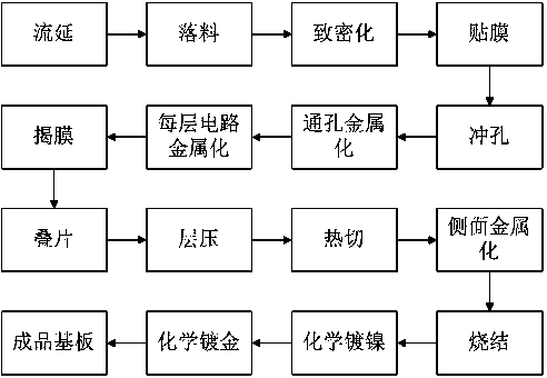
[0047] Using tape casting equipment at a drying temperature of 100°C, a single sheet of green porcelain tape with a thickness of 0.14mm and a length and width of 210mm was obtained. A single layer of aluminum nitride green ceramic tape with a thickness of 0.14mm was densified under a pressure of 1.0kpsi. Apply a film to the densified raw porcelain tape.

[0048] After the film is pasted, use mechanical punching equipment to punch through holes with a diameter of 0.2mm; use a screen printing machine to fill the tungsten paste into the through holes; after drying, use a screen printing machine to coat each layer with tungsten paste The circuit is printed; after drying, each layer of green ceramic tape is peeled off and stacked in order, and 8 layers of green ceramic tape are combined under a pressure of 1.50kpsi by isostatic pressing; hot cutting is carried out according to the marking line by a hot cutting machine to obtain unit, and each unit sidewall is fully metallized with...


PUM

PropertyMeasurementUnit
thicknessaaaaaaaaaa
thicknessaaaaaaaaaa

Abstract

The invention relates to a multi-layer aluminum nitride substrate for highly integrated module level packaging, and a manufacturing method thereof. The structure of the substrate comprises upper and lower surface layers, wherein the upper and lower surface layers are high-precision and high-density metalized welding pads; the side walls of the substrate are fully metalized; and the substrate is internally provided with multi-layer metalized wiring. The upper and lower surface layer metalized welding pads are welded with ball gates of a silicon-based chip; the side walls are fully metalized torealize signal shielding; the multi-layer metalized wiring inside the substrate satisfies complicated circuit signal transmission and interconnection. By utilizing a multi-layer co-firing process, aluminum nitride ceramic is selected as the ceramic base body material, tungsten is used as the metallization material, a green tape binding micro-deformation process adopted, and a tungsten metal circuit layer on the surface layer is plated by adopting chemical nickel-plating and chemical gilding processes. The multi-layer aluminum nitride substrate and the manufacturing method thereof have the advantages that the aluminium nitride substrate and the silicon-based chip are highly matched in coefficients of thermal expansion, and the reliability of ball gate welding packaging of the silicon-basedchip is realized; and the thermal conductivity of the substrate is increased to 170 W/mK, thereby being capable of meeting the high power density packaging and heat dissipation requirements of the highly integrated module.

Description

technical field [0001] The invention relates to a multilayer aluminum nitride substrate for highly integrated module-level packaging and a manufacturing method thereof, belonging to the technical field of electronic packaging. Background technique [0002] With the continuous miniaturization and high integration of electronic devices, the number of chips and output power per unit volume of the device continue to increase, which puts forward higher performance requirements for ceramic substrates for packaging. Especially module-level packaging, a large number of chips in the module, high unit power density, requires the substrate to provide good heat dissipation requirements and a good thermal expansion coefficient matching with the chip, to avoid reliability problems when the chip is working. [0003] For polymer substrates, due to their low cost and easy molding, they are most widely used in the field of packaging and interconnection. However, its thermal conductivity is l...

Claims


Application Information

Patent Timeline
Patent Type & Authority Applications(China)
IPC IPC(8): H01L23/498H01L21/48H01L23/367
CPCH01L21/4857H01L23/367H01L23/49805H01L23/49822H01L23/49838
Inventor 陈寰贝陈骏夏庆水
Owner NO 55 INST CHINA ELECTRONIC SCI & TECHNOLOGYGROUP CO LTD
Why Eureka
Try Eureka