Quantum-dot light-emitting diode and preparation method thereof

A quantum dot light-emitting and diode technology, used in semiconductor/solid-state device manufacturing, semiconductor devices, electrical components, etc., can solve problems such as low carrier recombination efficiency, insufficient hole injection, and reduced quantum yield, to avoid quantum Yield drop, reduced quantum yield drop, effect of slowing down electron injection rate

Pending Publication Date: 2019-03-29
HENAN UNIVERSITY +1
View PDF9 Cites 22 Cited by
  • Summary
  • Abstract
  • Description
  • Claims
  • Application Information

AI Technical Summary

Problems solved by technology

[0003] The fundamental reason for the low efficiency and lifespan of blue QLED devices in the past is that when using conventional organic-inorganic hybrid QLED device structures to construct blue QLEDs, due to the presence of quantum dots between the inorganic hole injection layer and the quantum dot light-emitting layer, compared to the red and green quantum The larger injection b

Method used


Image

  • Quantum-dot light-emitting diode and preparation method thereof
  • Quantum-dot light-emitting diode and preparation method thereof
  • Quantum-dot light-emitting diode and preparation method thereof

Examples


preparation example Construction

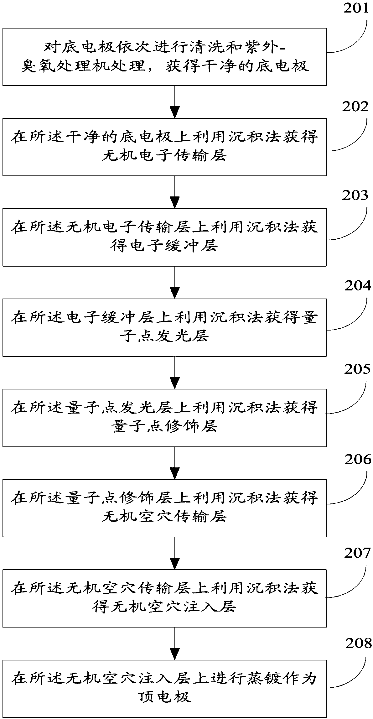
[0061] figure 2 It is a flow chart of the method for preparing quantum dot light-emitting diodes according to the embodiment of the present invention, such as figure 2 shown. The preparation method of quantum dot light-emitting diode specifically comprises the following steps:

[0062] Step 201: Cleaning the bottom electrode 1 and treating it with an ultraviolet-ozone processor in sequence to obtain a clean bottom electrode 1; specifically:

[0063] Clean the bottom electrode 1 of the glass or PET film substrate containing the ITO electrode with pure water, acetone and isopropanol for 10-30 minutes respectively.

[0064] Use ultraviolet-ozone treatment machine (UV / O to the bottom electrode 1 after cleaning) 3 ) for further cleaning for 10 to 30 minutes to obtain a clean bottom electrode 1 .

[0065] In the present invention, cleaning with pure water, acetone and isopropanol for the first time is to remove the particle impurities on the surface, and the second time uses t...

Embodiment 1

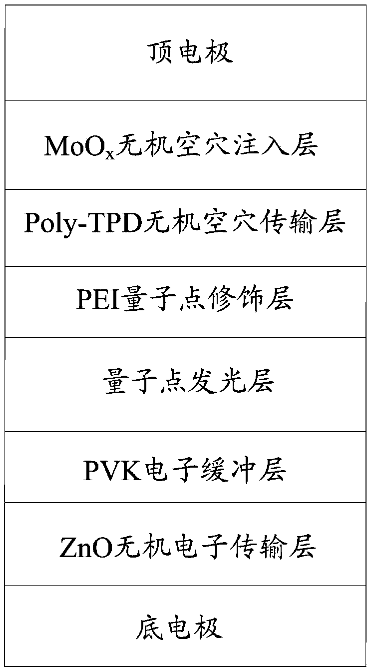
[0092] image 3 For the embodiment of the present invention, PVK is used as the electronic buffer layer 3, and PEI is used as the quantum dot light-emitting diode of the quantum dot modification layer 5, such as image 3 shown. A glass substrate with an ITO electrode was used as the bottom electrode 1, and the bottom electrode 1 was sequentially treated with pure water, acetone, isopropanol, and an ultraviolet-ozone processor (UV / O 3 ) treatment, each treatment for 15 minutes, to remove impurities and organic matter on the residual glass surface, and improve the work function of ITO; then use the spin coating method to prepare a 100nm thick ZnO thin film on the clean bottom electrode 1 containing the ITO electrode side As the inorganic electron transport layer 2 (ZnO dissolved in absolute ethanol, the solution concentration is 60 mg / ml, the spin coating speed is 2000 rpm, and the spin coating time is 60 seconds), the ZnO thin film is dried in a glove box at 60 °C 5min to rem...

Embodiment 2

[0094] Figure 5 For the embodiment of the present invention, TFB is used as the electronic buffer layer 3, and PEIE is used as the quantum dot light-emitting diode of the quantum dot modification layer 5, such as Figure 5 shown. A glass substrate with an ITO electrode was used as the bottom electrode 1, and the bottom electrode 1 was sequentially treated with pure water, acetone, isopropanol, and an ultraviolet-ozone processor (UV / O 3 ) treatment, each treatment for 15 minutes, to remove impurities and organic matter on the residual glass surface, and improve the work function of ITO; then utilize the spin coating method to prepare a 100nm thick ZnMgO thin film on the clean bottom electrode 1 containing the ITO electrode side As the inorganic electron transport layer 2 (ZnMgO dissolved in absolute ethanol, the solution concentration is 60 mg / ml, the spin coating speed is 2000 rpm, and the spin coating time is 60 seconds), the ZnMgO film is dried in a glove box at 60 °C 5mi...


PUM

PropertyMeasurementUnit
Thicknessaaaaaaaaaa
Thicknessaaaaaaaaaa
Thicknessaaaaaaaaaa

Abstract

The invention discloses a quantum-dot light-emitting diode and a preparation method thereof. The quantum-dot light-emitting diode comprises an inorganic electron transport layer, an electron buffer layer, a quantum dot light-emitting layer, a quantum dot modification layer and an inorganic hole transport layer. The electron buffer layer is disposed on the upper side of the inorganic electron transport layer; the quantum dot light-emitting layer is arranged at the upper side of the electron buffer layer; the quantum dot modification layer is arranged at the upper side of the quantum dot light-emitting layer; and the inorganic hole transport layer is arranged at the upper side of the modification layer. According to the invention, since the electron buffer layer is arranged between the inorganic electron transport layer and the quantum dot light-emitting layer and the quantum dot modification layer is arranged between eh inorganic hole transport layer and the quantum dot light-emitting layer, the damages on the quantum dot light-emitting layer by the inorganic electron transport layer and the inorganic hole transport layer can be reduced effectively, the luminous quantum yield of thequantum dot light-emitting layer is increased, and the carrier injection efficiency is modulated; the quantum dot light-emitting layer can be protected; the device is protected from being oxidized; the efficiency, service life and stability of the blue QLED are enhanced.

Description

technical field [0001] The invention relates to the technical field of electronic display, in particular to a quantum dot light-emitting diode and a preparation method. Background technique [0002] Quantum dot-based electroluminescent devices (QLEDs) utilize stable inorganic fluorescent quantum dots as the light-emitting active layer, and have superior characteristics such as precisely tunable saturated colors. Research on wide-color gamut light-emitting devices has shown that quantum dot light-emitting materials have more obvious advantages than traditional organic light-emitting diodes (OLEDs) and LCDs. Since the first report of QLED in 1994, research in this area has quickly attracted people's attention. After years of continuous development, the luminous brightness and luminous efficiency of QLED have been greatly improved compared with the early stage, and it has become more and more clear that it is a new generation. Possibility of light-emitting display devices. Ac...

Claims


Application Information

Patent Timeline
IPC IPC(8): H01L51/50H01L51/56
CPCH10K50/115H10K50/18H10K71/00
Inventor 申怀彬纪文宇李林松
Owner HENAN UNIVERSITY
Why Eureka
Try Eureka